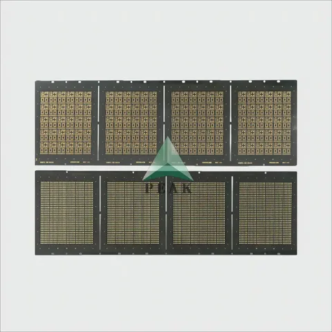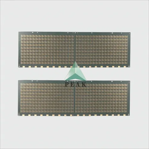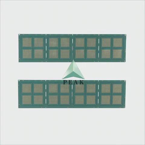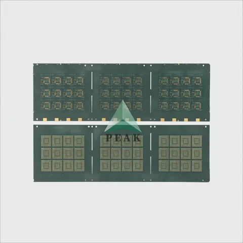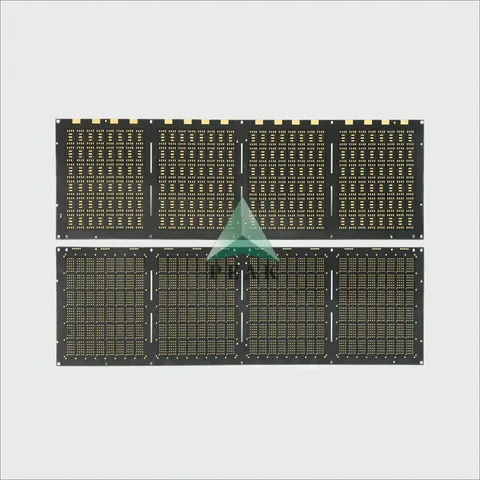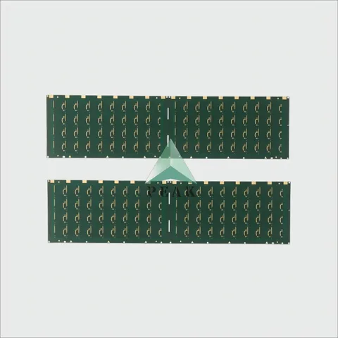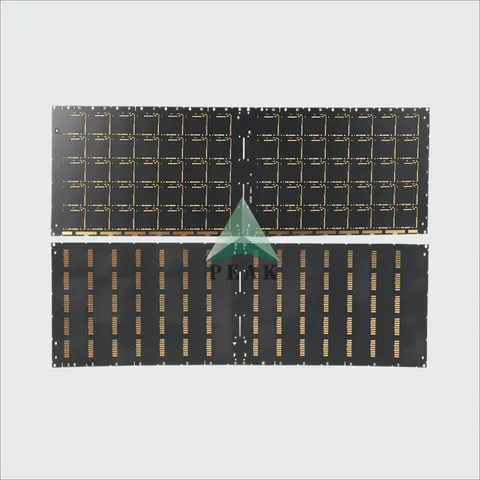
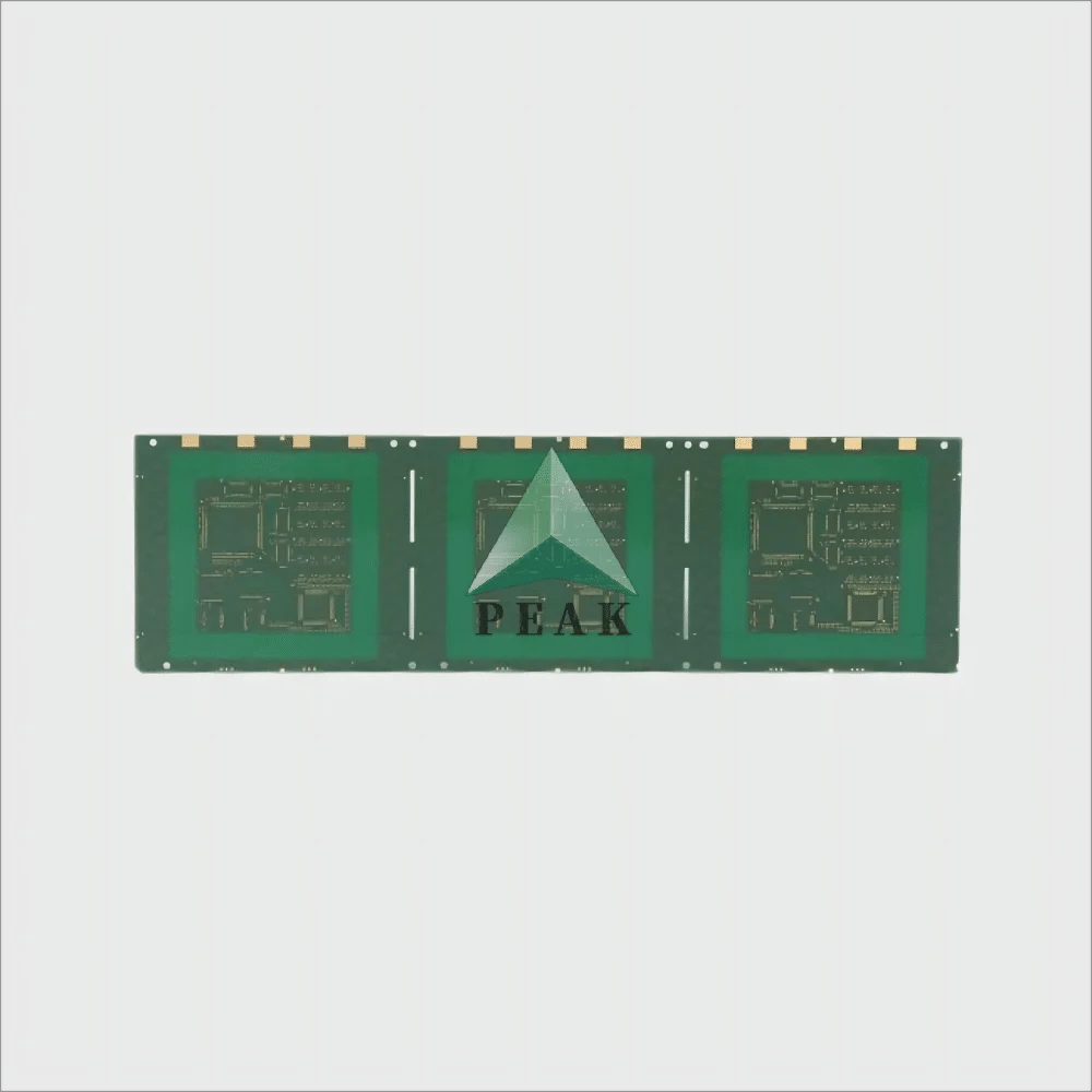
9 boards in this category

SUB PCB manufacturer

Sequential lamination decides which nets can be routed at all. These structures are released for mass production, not just prototype runs.

SUB PCB built by PEAK PCB in Shenzhen

Process window

  • CSP / FC-CSP / SiP / FC-BGA / WB-CSP
  • FR4 / BT / high-speed material
  • Trace width and space 12 / 12 μm
  • Solder mask registration ±20 μm
  • Strict solder mask flatness control ≤ 5 μm
Substrate and Substrate-Like PCB detail

What this category was actually built to

Ranges below are computed from the 9 boards listed on this page, not from a marketing sheet.

Built toRange across this category
Layer counts built2–6
Base materialsAMC832-HF, BT, EM-526, HL832N, MITSUBISHI GAS HL832NXA, SYTech Sl10U, SYTech Sl643HU
Surface finishesENEPIG, ENIG 2u, Hard Gold Body
Solder mask coloursBlack, Green
Finished thickness0.2–0.5 mm

9 SUB PCB builds

Need sub pcb quoted?

Send Gerber plus a drill file and a stack-up note. Quotation comes back within 6 hours, with DFM comments attached.