
Industry
IC Substrate and Packaging PCB
Substrate-like carriers for CSP, FC-BGA and SiP packages, where the tolerance stack is measured in microns across the whole array.

What this application demands of the board
Trace width and space to 12 / 12 μm
Solder mask registration ±20 μm
Solder mask flatness ≤ 5 μm
BT and high-speed laminates from MGC and Doosan
Categories used for ic substrate and packaging
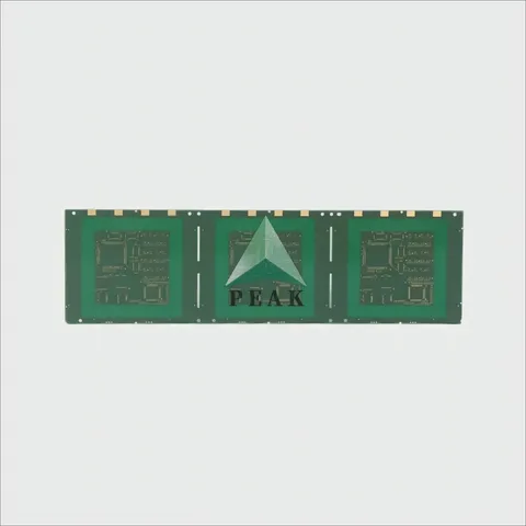
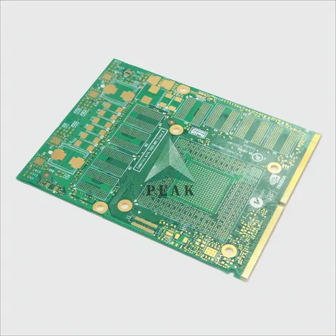
Examples from production
SUB PCB
EM-526 6 Layers 0.5mm Thickness Hoz ENEPIG Advanced BGA Substrate PCB
- Layers6 Layers (Max 64 Layers)
- Base materialEM-526
- Finished thickness0.5 mm (Max 8mm)
Multilayer PCB
10 Layers Buried Resistance ENIG+Hard Gold (Gold Finger) POFV Multilayer PCB
- Layers10 Layers (Max 64 Layers)
- Base materialTU 768
- Finished thickness2.0 mm (Max 8mm)
Building for ic substrate and packaging?
Send the requirement — dielectric, thermal, qualification standard — and we will come back with a manufacturable stack-up and a price.