
Blind, buried and hybrid via structures
HDI PCB
High-density interconnect is a stack-up problem before it is a drilling problem; we build the sequential lamination that the routing actually needs.
Published capability limits
- Blind / buried / hybrid via
- 5+N(N+M)+5 structure
- Trace width and spacing 1.6 / 1.6 mil
- Laser hole size ≥ 0.075 mm
- High density interconnector

Categories that sit inside this window
6 catalogue categories, 64 boards in total.
Representative builds
HDI PCB
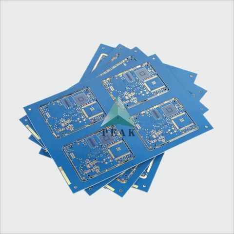
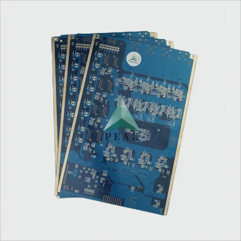
High TG ISOLA 370HR 8 Layers Buried Via(L4-L5) Edge Plating Blue HDI PCB
- Layers8 Layers (Max 64 Layers)
- Base materialISOLA 370HR
- Finished thickness1.6 mm (Max 8mm)
Blind/Buried Via
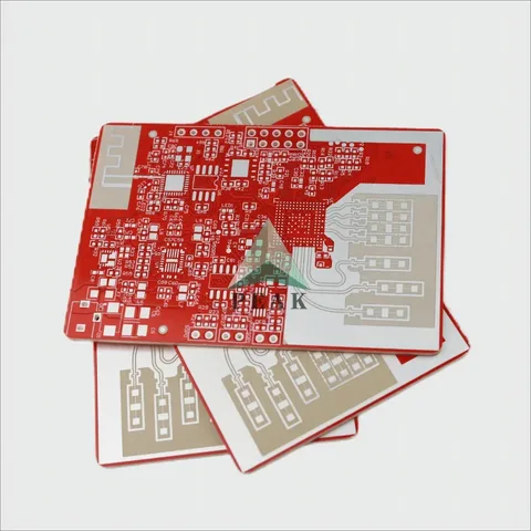
Rogers Ro3003+ISOLA 370HR Hybrid Lamination Blind Via mm Wave Radar PCB
- Layers6 Layers (Max 64 Layers)
- Base materialRogers Ro3003+ISOLA 370HR
- Finished thickness1.5 mm (Max 8mm)
Multilayer PCB
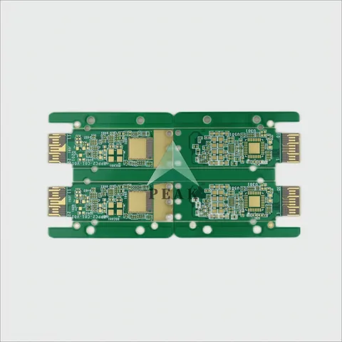
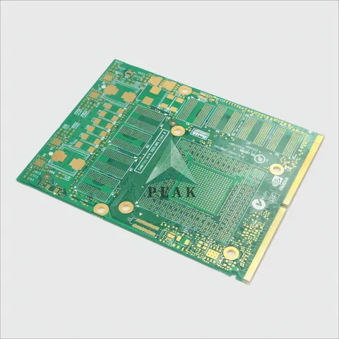
10 Layers Panasonic Megtron6 1+N+1 Structure (L1-4;L4-7;L7-10) ENIG HDI High Speed PCB
- Layers10 Layers (Max 64 Layers)
- Base materialPanasonic Megtron 6
- Finished thickness2.0 mm (Max 8mm)
HDI PCB
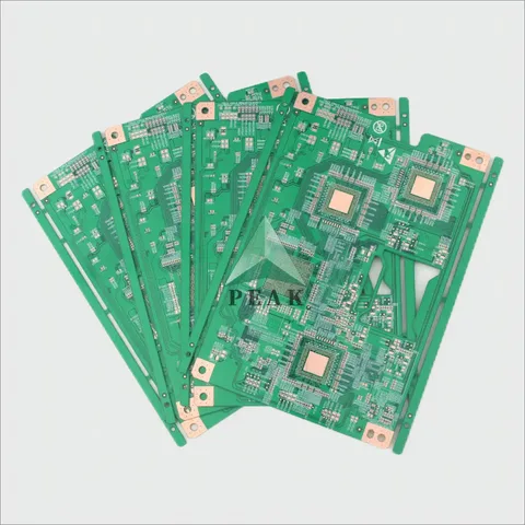
10 Layers OSP 2+N+2 Structure (L1-2;L1-4;L4-7;L7-10;L9-10) Advanced HDI PCB
- Layers10 Layers (Max 64 Layers)
- Base materialFR4 TG170
- Finished thickness2.0 mm (Max 8mm)
HDI PCB quoted in 6 hours
Gerber plus a stack-up note is enough to start. If the design sits outside the window above, we will say so and propose the change that brings it back in.