
Industry
Memory and Storage PCB
Memory sticks, USB drives and storage carriers where gold finger construction and outline accuracy decide the insertion life of the part.
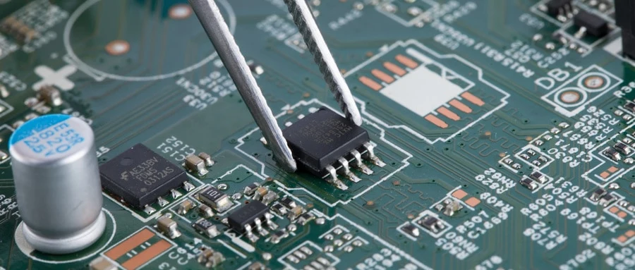
What this application demands of the board
Hard gold up to 3.0 μm on fingers, selective plating
Step and segmented gold finger geometry
Plated half holes for module edge contacts
Bevelled edge (hypotenuse) at 20°, 30° or 45°
Categories used for memory and storage
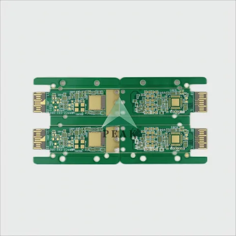
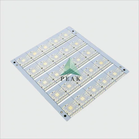
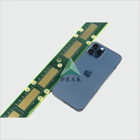
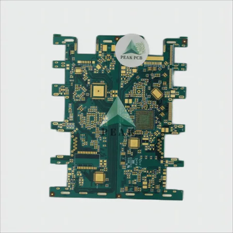
Examples from production
Multilayer PCB
10 Layers Panasonic Megtron6 1+N+1 Structure (L1-4;L4-7;L7-10) ENIG HDI High Speed PCB
- Layers10 Layers (Max 64 Layers)
- Base materialPanasonic Megtron 6
- Finished thickness2.0 mm (Max 8mm)
Metal Core PCB
Advanced Double Side Aluminum-Based Plated Half Holes ENIG 1u White PCB
- Layers2 Layers (Max 64 Layers)
- Base materialAluminum-Based
- Finished thickness1.6 mm (Max 8mm)
2 Layers PCB
7.8 mm Ultra-Thick Counterboring Double Side Immersion Gold 1u PCB
- Layers2 Layers (Max 64 Layers)
- Base materialFR4 TG135
- Finished thickness7.8 mm (Max 8mm)
Multilayer PCB
Fully Halogen Free Production 4 Layers POFV Immersion Gold 1u Multilayer PCB
- Layers4 Layers (Max 64 Layers)
- Base materialIT150GSTC
- Finished thickness1.2 mm (Max 8mm)
Building for memory and storage?
Send the requirement — dielectric, thermal, qualification standard — and we will come back with a manufacturable stack-up and a price.