What this category was actually built to
Ranges below are computed from the 32 boards listed on this page, not
from a marketing sheet.
Background
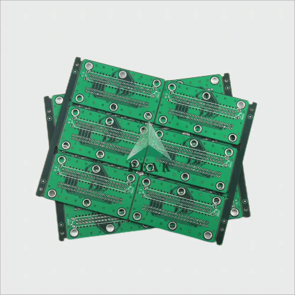
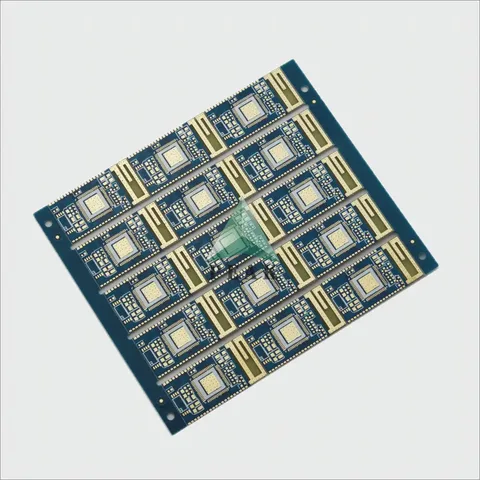
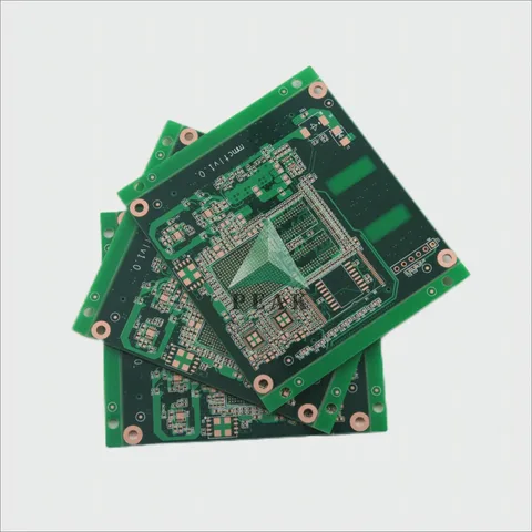
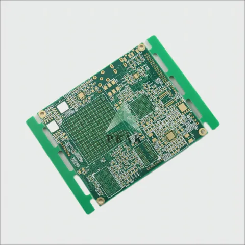
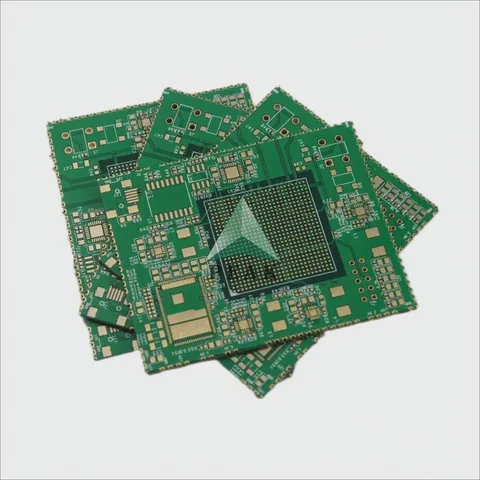
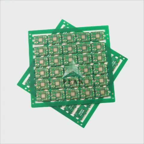
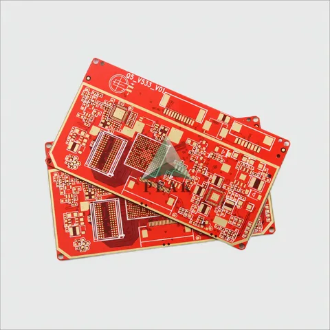
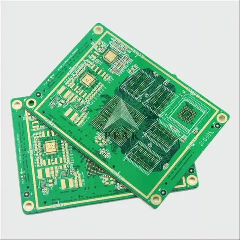
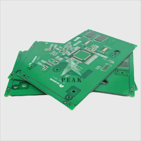
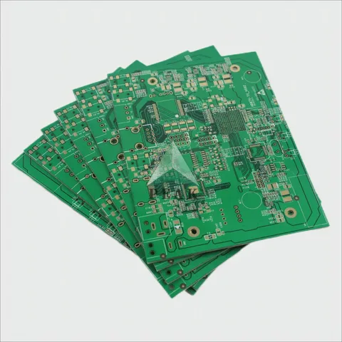
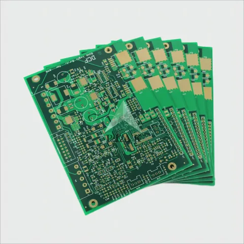
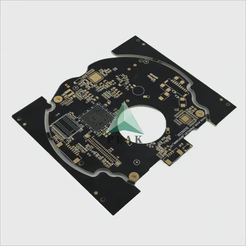
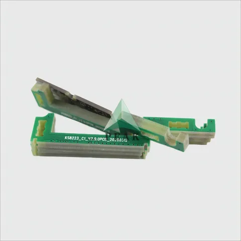
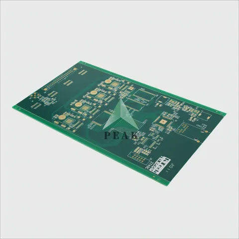
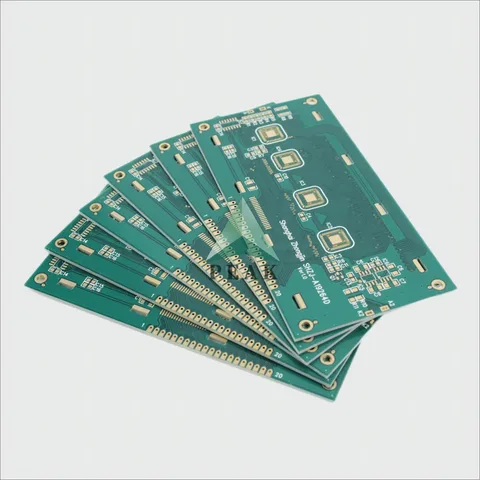
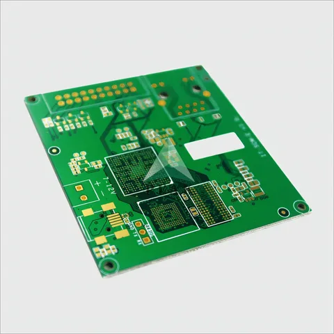
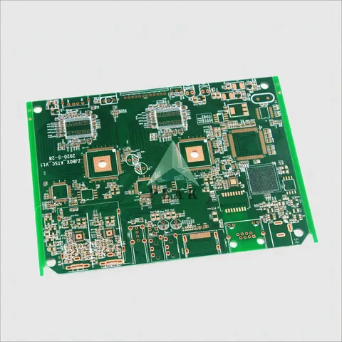
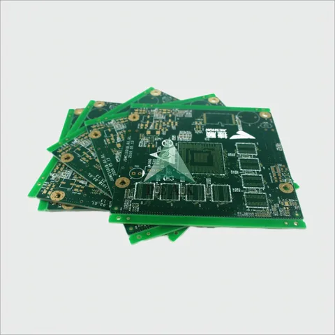
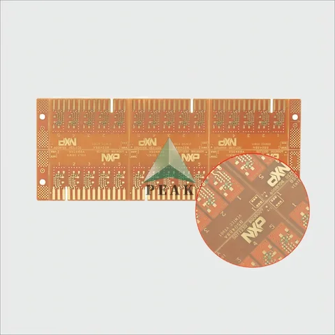
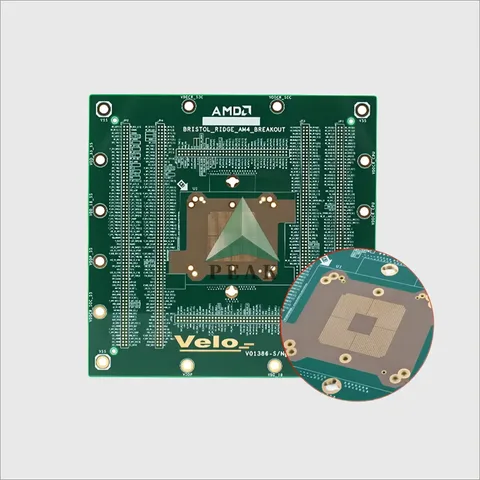
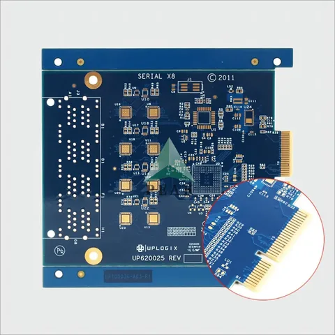
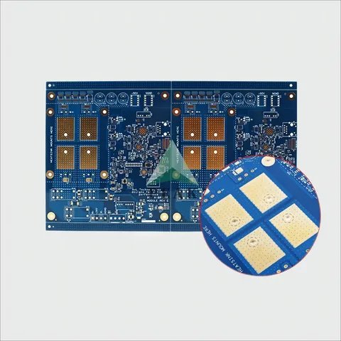
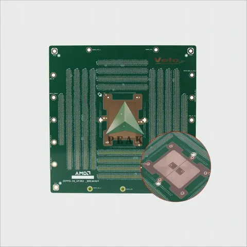
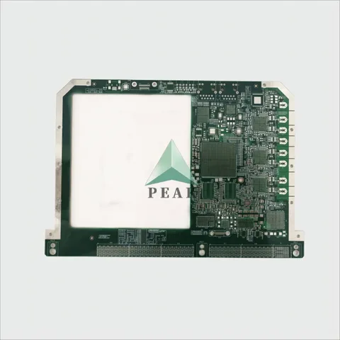
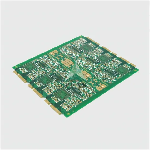
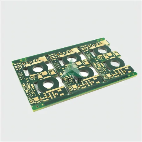
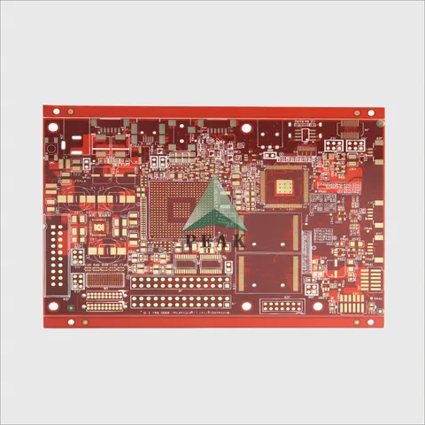
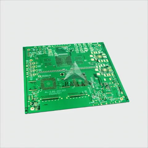
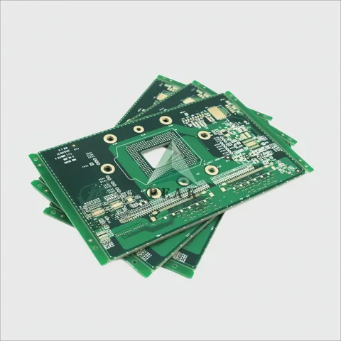
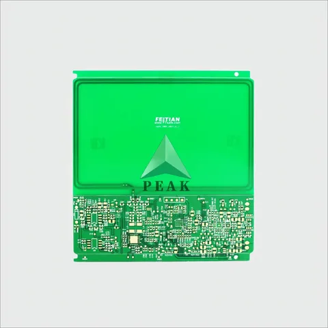
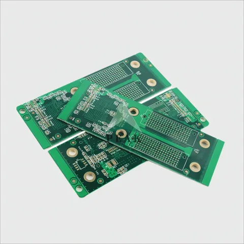
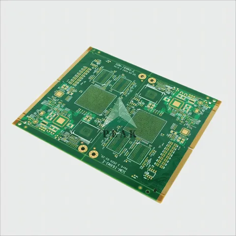
Multilayer PCB or Printed Circuit Board is a type of board which is used in electronic devices. As the name suggests, it consists of multiple layers of copper conducting paths that are separated by an insulating material called substrate. It is used in high-end electronic devices because of its advantages over the traditional single-layered PCBs.
Multilayer PCBs are made up of multiple layers of conducting paths and insulating materials. These layers are then laminated together to create a single board. The number of layers in a Multilayer PCB can vary depending on the application of the device. Some Multilayer PCBs can have up to 30-40 layers, whereas others may have fewer layers.
The biggest advantage of Multilayer PCBs is their ability to handle complex circuits and designs. Single-layered PCBs have a limited number of components that can be placed on them. However, Multilayer PCBs can accommodate a higher number of components because of their multiple layers. This makes it possible to design more advanced electronic devices.
Multilayer PCBs are also more reliable and durable than single-layered PCBs. The multiple layers provide additional support and stability to the board, making it less prone to damage. The insulating substrate material used in Multilayer PCBs is also more heat-resistant and can withstand higher temperatures without degrading.
Another advantage of Multilayer PCBs is their ability to reduce electromagnetic interference (EMI). The multiple layers of conducting paths in Multilayer PCBs allow for better shielding of the components, reducing EMI. This is particularly important in sensitive electronic devices where EMI can cause interference and disrupt the functioning of the device.
In conclusion, Multilayer PCBs are a superior alternative to traditional single-layered PCBs. They offer the ability to handle complex circuits, are more reliable and durable, and can reduce electromagnetic interference. Multilayer PCBs are widely used in high-end electronic devices such as smartphones, laptops, and other advanced electronic devices.