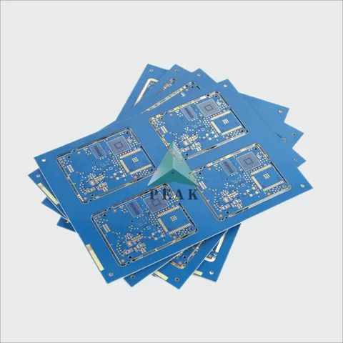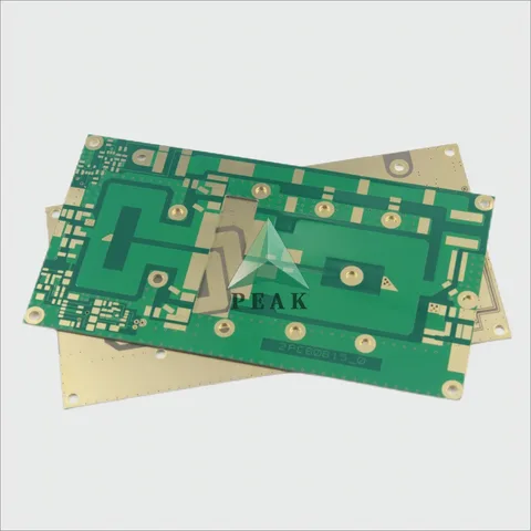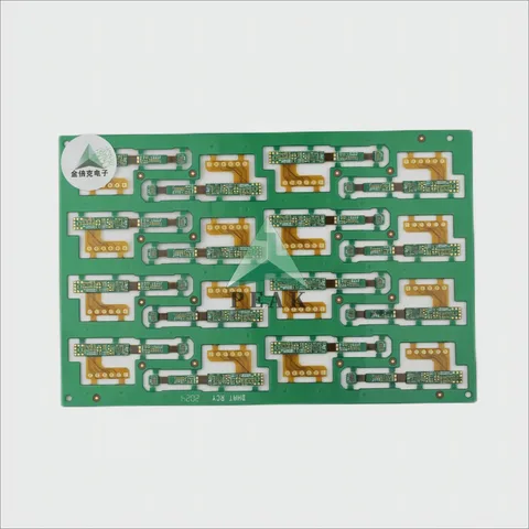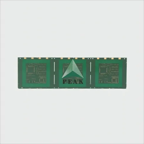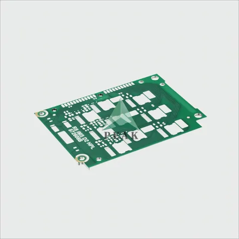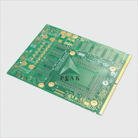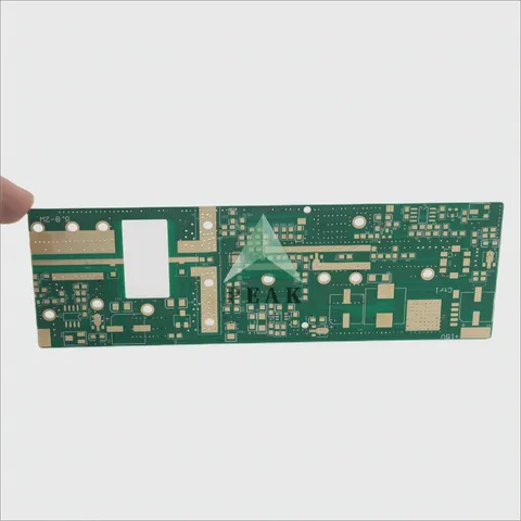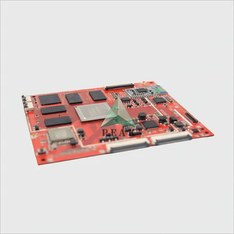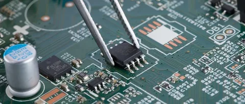

FR4 stacks up to 64 layers
Regular Rigid PCB
- Up to 64 layers
- FR4 TG135 / TG150 / TG170
- Halogen free / CTI ≥ 600
- Aspect ratio (finished hole) 28:1
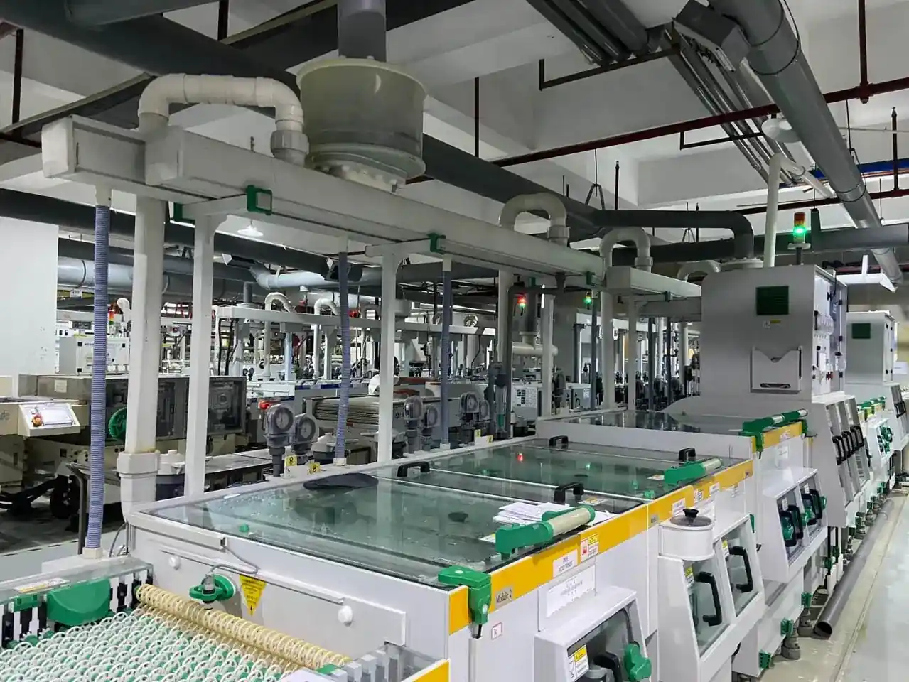
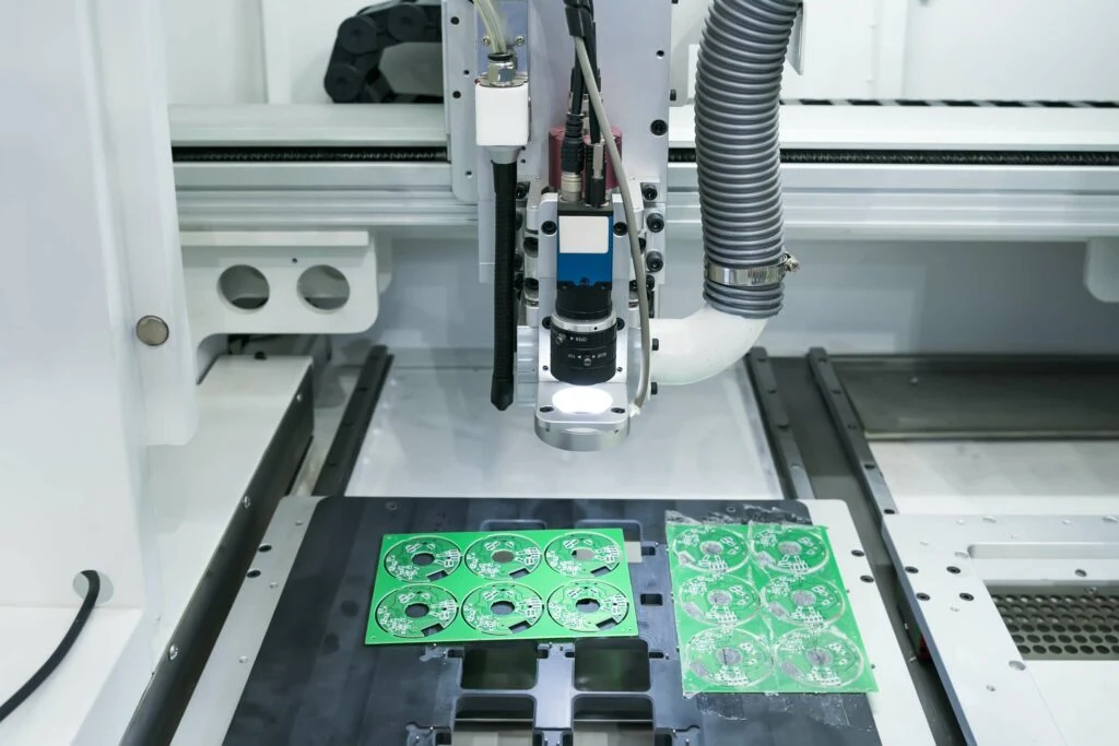

Rigid, rigid-flex, HDI and substrate — one plant
1 to 64 layers fabricated, assembled, tested and validated in a 54,000 m² Shenzhen plant — so a stack-up change does not mean changing suppliers.
Expedited samples in as little as 8 hours
Quick-turn fabrication plus turnkey PCBA
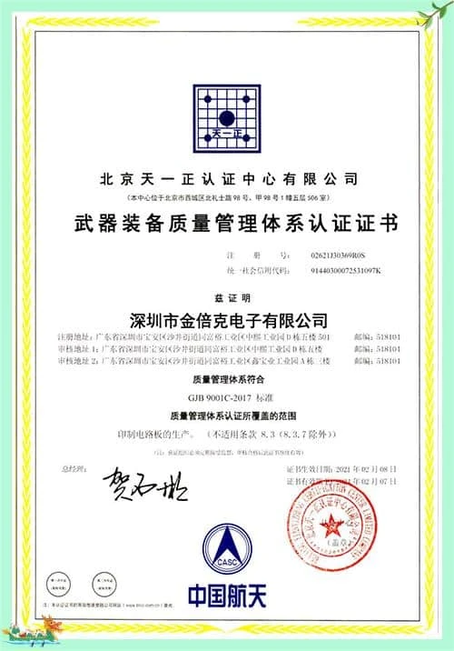
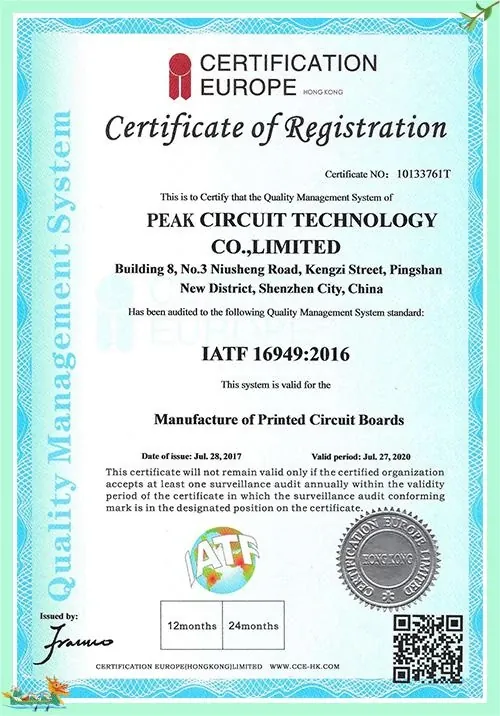
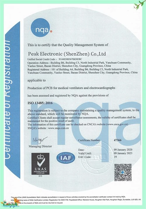
Bare board, stencil, SMT, DIP, ICT and FCT testing from one purchase order, under GJB9001C military, IATF 16949 and ISO 13485 certified systems.
Down to 2 mil trace, 0.075 mm laser via
The boards other shops quote as not manufacturable
HDI up to 5+N(N+M)+5, hybrid lamination, buried capacitance, POFV, backdrill and step gold finger — released for mass production, not just prototypes.
Why engineers move a programme here
PEAK was founded in Shenzhen in 2007 and now fabricates 1–64 layer rigid, rigid-flex, HDI, high-frequency, high-speed, metal-core and IC-substrate boards, then assembles and tests them in the same facility.
OEM engineering teams in aerospace and defense, medical, semiconductor test, telecom infrastructure, automotive and industrial control — the projects where a board is qualified once and then has to be reproducible for years.
Designs that fail DFM at ordinary shops: 18-layer stacks, Rogers-plus-FR4 hybrid lamination, 2 mil trace and space, 0.075 mm laser vias, 14 oz copper, CTI ≥ 600 and plated half holes on the same panel.
Fabrication, stencil, assembly and electrical test sit in the same 54,000 m² plant, so impedance coupons, slice analysis and flying-probe results come back to one engineering team instead of crossing three vendors.
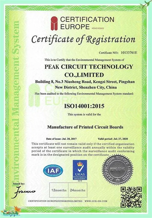
GJB9001C military certification, IATF 16949, ISO 13485, ISO 9001, ISO 14001, UL and CQC approvals; 11 granted production patents; 45+ engineers; shipments to 190+ countries since 2007.
Construction types
These are the capability limits the plant actually runs to. Pick the closest one and the detail page lists the material sets and the boards already built against it.
Built and shipped
Every listing carries the stack-up, material, geometry and finish it was manufactured to — 150 of them, across 47 categories.
Proof, not adjectives

How a job runs
45+ engineers review DFM, stack-up and impedance targets before tooling starts.
Expedited 1–2 layer samples; multilayer and HDI samples on a quoted schedule.
Industries
Controllers, drives and motherboards that have to survive a factory floor for a decade and stay buildable from the same data package.
Transceiver boards where insertion loss budget and mechanical registration are decided by the laminate and the etch, not by the layout.
Automotive and industrial radar front ends built on specified PTFE and ceramic-filled laminates, with blind vias placed to keep the feed network clean.
Substrate-like carriers for CSP, FC-BGA and SiP packages, where the tolerance stack is measured in microns across the whole array.
Infrastructure boards that combine an RF section, a high-speed digital section and a power section on one panel — usually as a hybrid stack.
Memory sticks, USB drives and storage carriers where gold finger construction and outline accuracy decide the insertion life of the part.
Knowledge base
PCB stackup refers to the arrangement of layers on a printed circuit board (PCB), including conductors, dielectric layers and any necessary components. It plays an integr…
HDI PCB (High-Density Interconnect Printed Circuit Board) is an increasingly popular type of printed circuit board due to its numerous benefits for modern electronics des…
Surface finish of printed circuit boards (PCBs) plays a critical role in its overall performance, reliability and solderability. A properly selected surface finish protec…
Quotation inside 6 hours, DFM feedback with it. No forms — email or WhatsApp reaches the engineering team directly.