
Industry
5G Base Stations PCB
Infrastructure boards that combine an RF section, a high-speed digital section and a power section on one panel — usually as a hybrid stack.

What this application demands of the board
Hybrid lamination of RF and FR4 material, 4–48 layers
Megtron 4 / 6 / 7 and FR408HR for the digital section
POFV and backdrill for via stub control
Large format panels up to 609 × 1200 mm
Categories used for 5g base stations
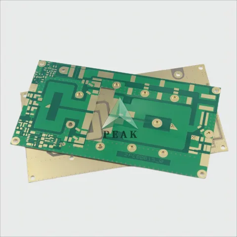
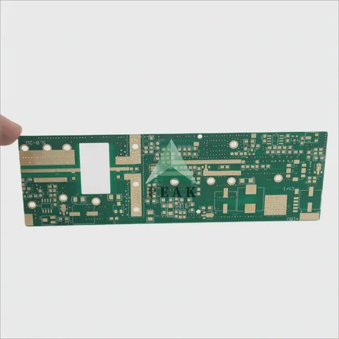
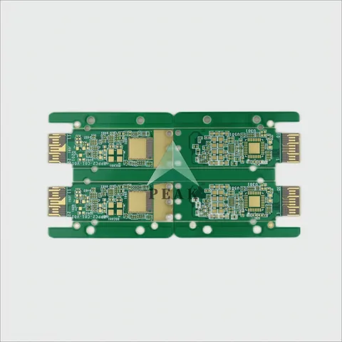
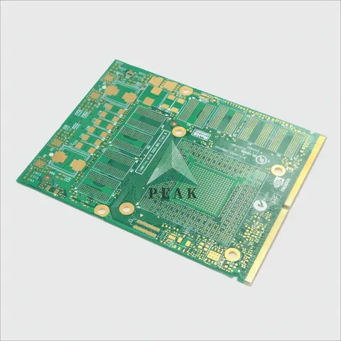
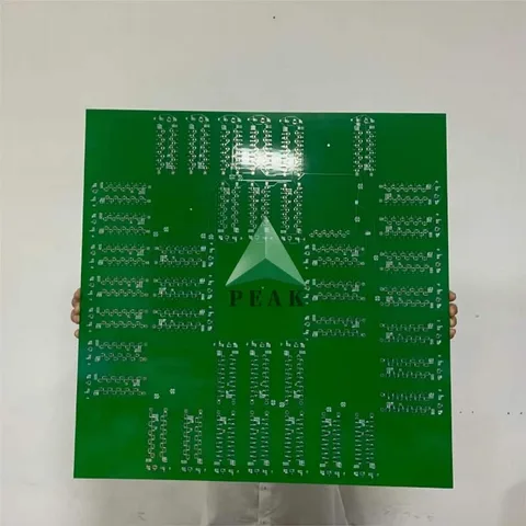
Examples from production
High Frequency PCB
ITEQ IT150DA (DK3.56; DF0.0047) Double Side Immersion Gold 1u PCB
- Layers2 Layers (Max 64 Layers)
- Base materialITEQ IT150DA
- Finished thickness1.0 mm (Max 8mm)
High Speed PCB
EMC-EM828 (DK3.7; DF0.008)+FR4 ISOLA370HR 4 Layers Hybrid Lamination PCB
- Layers4 Layers (Max 64 Layers)
- Base materialEMC-EM828 + ISOLA370HR
- Finished thickness1.6 mm (Max 8mm)
Multilayer PCB
10 Layers Panasonic Megtron6 1+N+1 Structure (L1-4;L4-7;L7-10) ENIG HDI High Speed PCB
- Layers10 Layers (Max 64 Layers)
- Base materialPanasonic Megtron 6
- Finished thickness2.0 mm (Max 8mm)
Multilayer PCB
10 Layers Buried Resistance ENIG+Hard Gold (Gold Finger) POFV Multilayer PCB
- Layers10 Layers (Max 64 Layers)
- Base materialTU 768
- Finished thickness2.0 mm (Max 8mm)
Building for 5g base stations?
Send the requirement — dielectric, thermal, qualification standard — and we will come back with a manufacturable stack-up and a price.