20 boards in this category

HDI PCB manufacturer

Sequential lamination decides which nets can be routed at all. These structures are released for mass production, not just prototype runs.

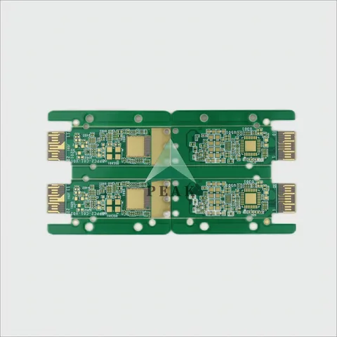
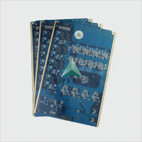
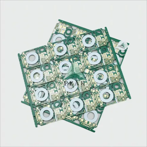
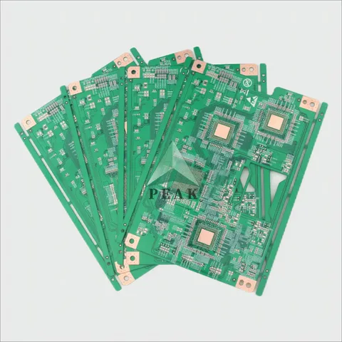
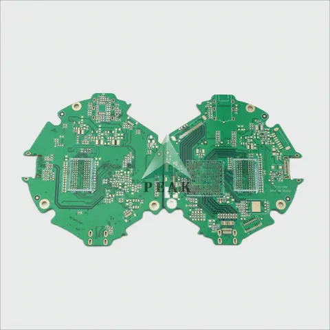
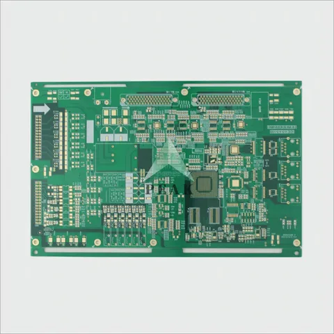
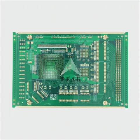
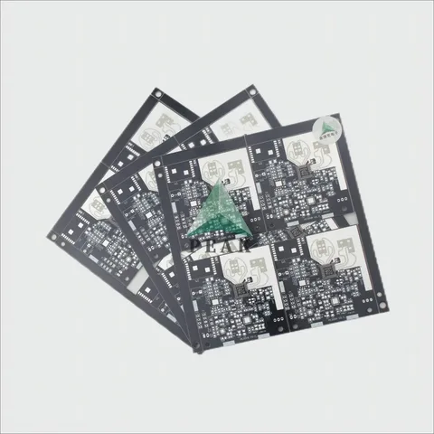
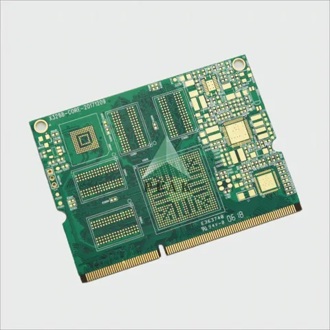
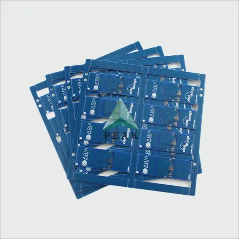
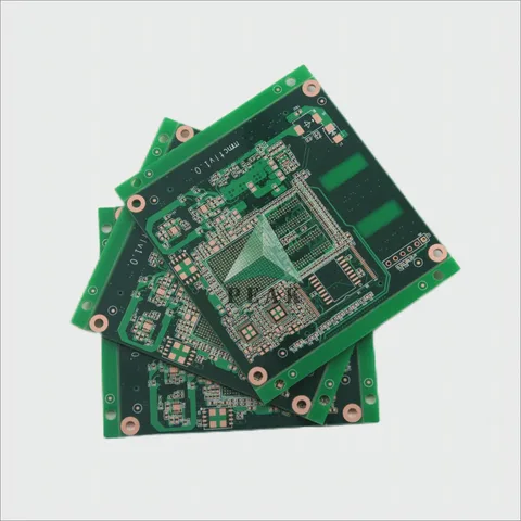
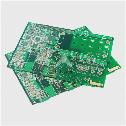
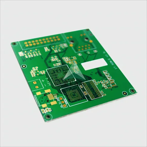
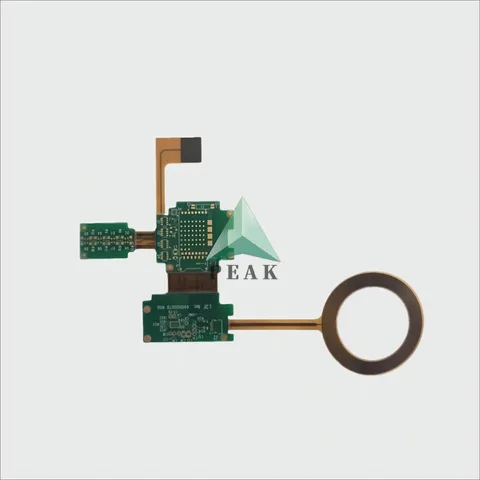
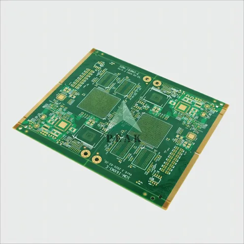
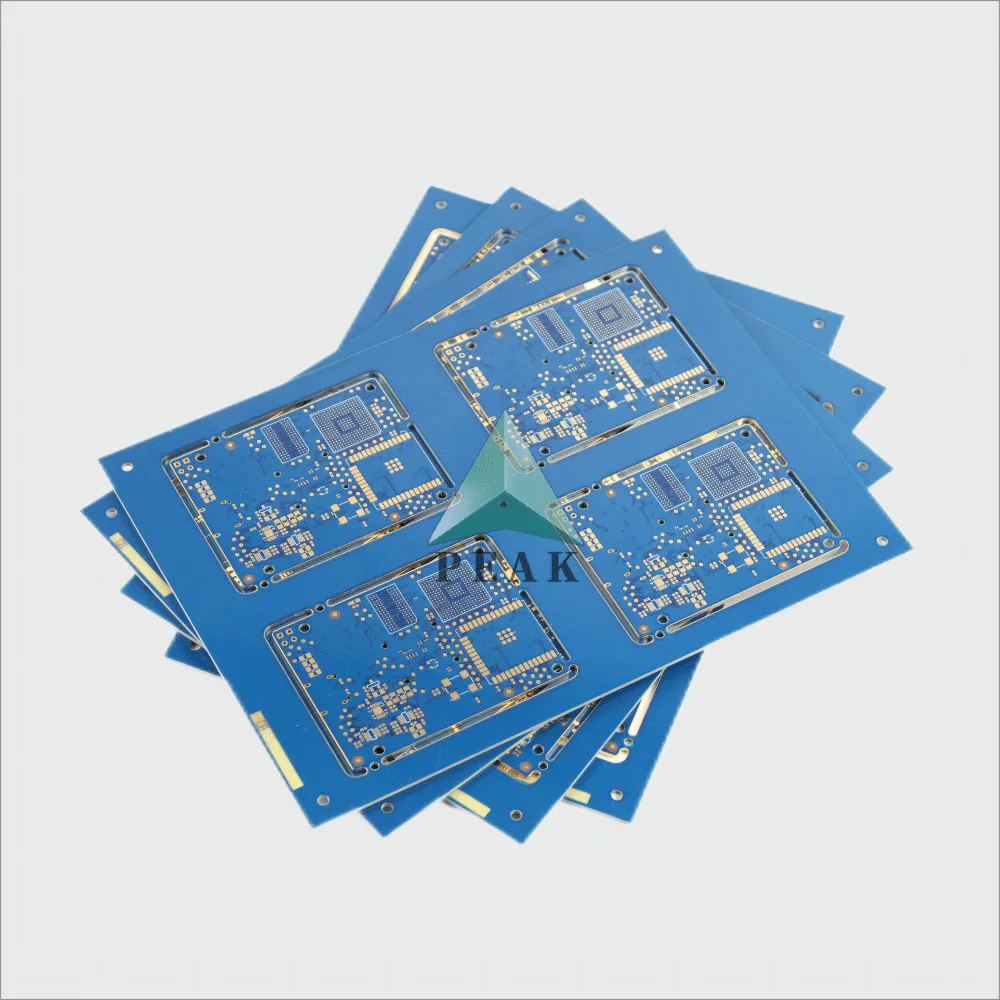
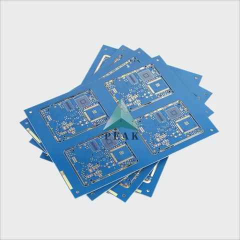
HDI PCB built by PEAK PCB in Shenzhen

Process window

  • Blind / buried / hybrid via
  • 5+N(N+M)+5 structure
  • Trace width and spacing 1.6 / 1.6 mil
  • Laser hole size ≥ 0.075 mm
  • High density interconnector
HDI PCB detail

What this category was actually built to

Ranges below are computed from the 20 boards listed on this page, not from a marketing sheet.

Built toRange across this category
Layer counts built4–18
Base materialsCTI≥600, FR4 IT180A, FR4 TG150, FR4 TG170, ISOLA 370HR, ISOLA FR408HR, Panasonic Megtron 6, Ro4835+FR4 IT180A
Surface finishesENIG & Hard Gold, ENIG 1u, ENIG 2u, Immersion Silver, OSP
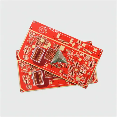
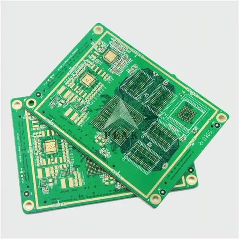
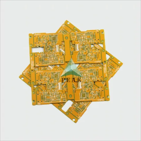
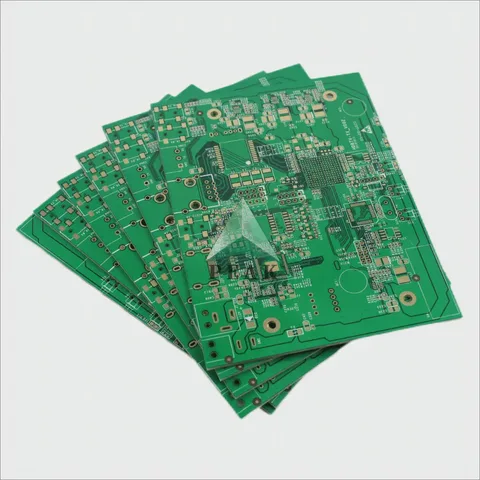
Solder mask coloursBlue, Green, Matte Black, Matte Green, Red, Yellow
Special processesBlind Via, Blind/Buried Via, Buried Capacitance, Edge Plating & Buried Via, POFV
Finished thickness1.2–3.6 mm

20 HDI PCB builds

Need hdi pcb quoted?

Send Gerber plus a drill file and a stack-up note. Quotation comes back within 6 hours, with DFM comments attached.