Metal Core PCB

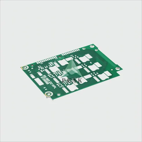
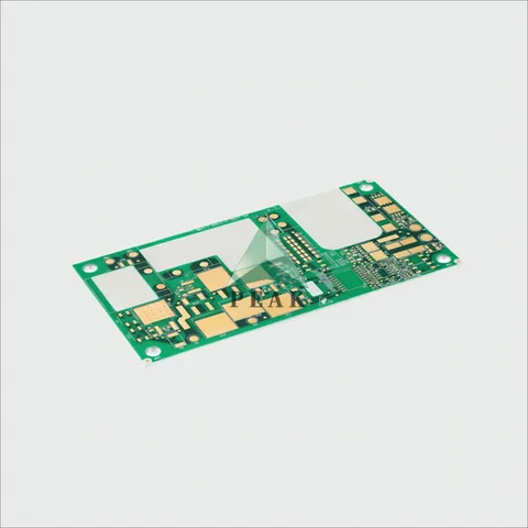
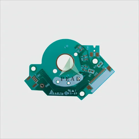
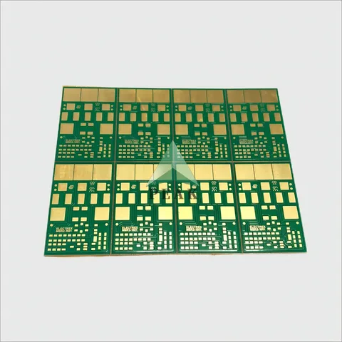
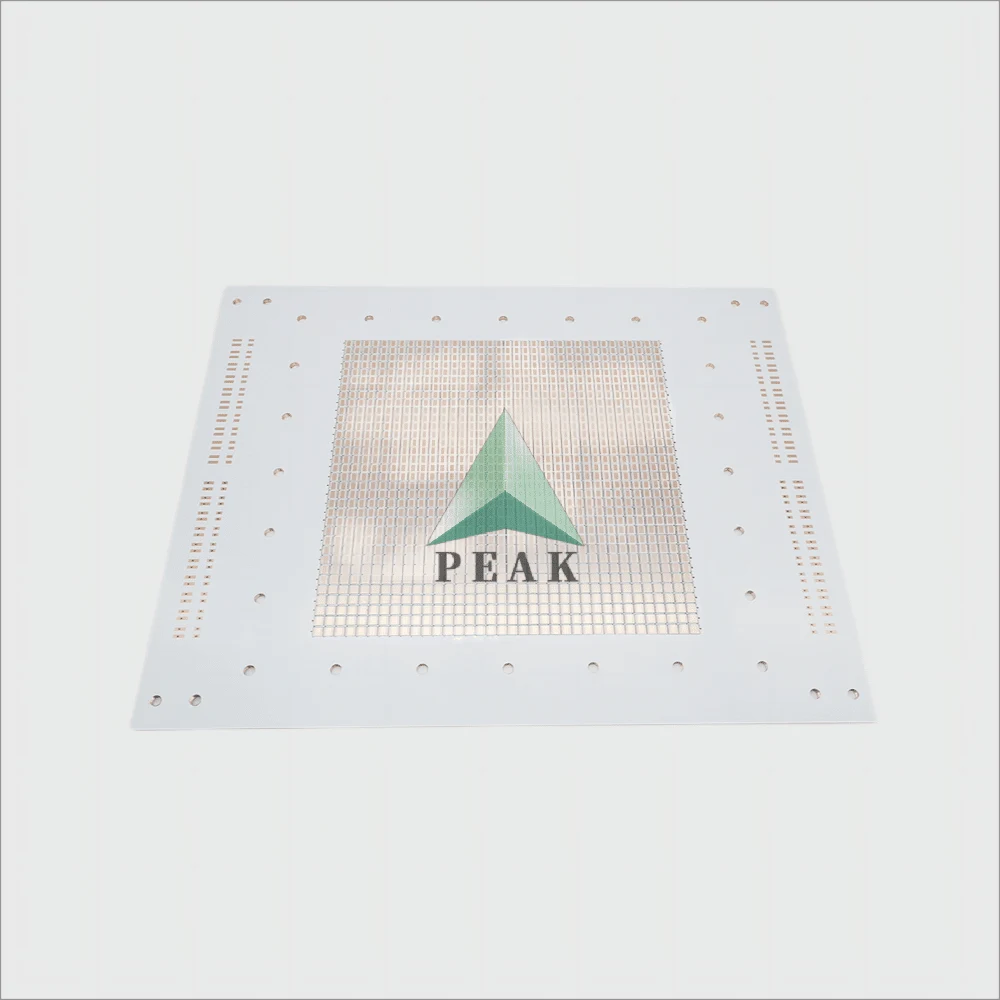
3.0w/m.k 1.6mm Thickness 2oz Copper-Thickness OSP AC3000V White PCB

This single-sided Copper-Based PCB is pressed on a copper base and finished at 1.6 mm overall thickness with OSP over white solder mask. What makes this part non-trivial: copper geometry held to 11.0 mil line width and 5.0 mil spacing, mechanical holes from 0.6 mm, finished copper at ½ oz / 2 oz. IPC-A-610 E Class II is the workmanship standard, verified by 100% AOI, ICT and FCT testing and thickness to ±10%. This one was quoted for electronic device.

  • LayersSingle Layer (Max 64 Layers)
  • Base materialCopper-Based
  • Finished thickness1.6 mm (Max 8mm)
  • Surface finishOSP
  • Min. line width / spacing11.0 mil (Min 2mil) / 5.0 mil (Min 2mil)

Quotation within 6 hours. Gerber, PowerPCB, CAD, AutoCAD, OrCAD, P-CAD, CAM-350 and CAM2000 files accepted.

What matters on this build

Single-sided construction, scalable to 64 layers

This part is single-sided; the same presses run 1 to 64 layers, so a stack-up revision does not force a supplier change.

Copper-Based laminate

Built on Copper-Based — copper base — drawn from over 120 laminate types held in the warehouse, from KB and ITEQ through Rogers, Isola and Panasonic.

11.0 mil / 5.0 mil line width and spacing

Etched to 11.0 mil width and 5.0 mil spacing here; the process floor is 2/2 mil inner at 1/3 oz copper, with ±10% accuracy on impedance layers.

OSP surface finish

Finished with OSP. ENIG 1–3 μin, ENEPIG, hard gold to 3.0 μm, immersion silver, immersion tin, OSP and lead-free HASL are all in-house.

Hole sizes from 0.6 mm mechanical

Drilling covers 0.15 mm mechanical and 0.076 mm laser holes, backdrill to ±0.1 mm and depth control to 0.05 mm.

Full specification as manufactured

These are the parameters this part was quoted, tooled and shipped against.

ParameterValue
PCB TypeCopper-Based PCB
Number of LayersSingle Layer (Max 64 Layers)
Finished Thickness1.6 mm (Max 8mm)
Base MaterialCopper-Based
Copper Thickness2oz
Min. Mechanical Hole0.6 mm (Min 0.1mm)
Min. Line Width11.0 mil (Min 2mil)
Min. Line Spacing5.0 mil (Min 2mil)
Surface FinishingOSP
Solder MaskWhite
Silk ScreenNo
Thickness Tolerance±10%
Impedance Control Accuracy±10% (min±5%)
Testing Service100% AOI ICT FCT Testing
Special ProcessesNo
PCB StandardIPC-A-610 E Class II
Brand NamePEAK PCB
Place of OriginShenzhen, Guangdong, China
Packaging InnerVacuum Packing/ Anti-Static Package
Packaging OuterExport Carton/ Customizable
PortShenzhen,Hongkong
Supply AbilitySample and Mass Production
Finished Inner Copper Thickness0oz (Max 14oz)
Finished Outer Copper Thickness2oz (Max 14oz)
Outline ProfileRout/ V-cut/ Bridge/ Stamp Hole
ApplicationElectronic Device
Acceptable File FormatGerber file, Powerpcb, CAD, AUTOCAD, ORCAD, P-CAD, CAM-350, CAM2000

Questions engineers ask about this board

Can this design be scaled beyond 1 layers?

Yes. This part is quoted at 1 layers and the plant fabricates 1 to 64 layers, including sequential-lamination HDI up to 5+N(N+M)+5.

Can a different laminate be substituted for Copper-Based?

It can. Copper-Based is what this part is built on, but material is a design input — Rogers, Arlon, Taconic, Isola, Nelco, Panasonic, TUC, ITEQ, SYTech, Ventec and KB grades are all stocked, and customer-supplied stock is accepted.

Is OSP the only surface finish offered on this board?

No. OSP is specified here; ENIG at 1–3 μin gold, ENEPIG, hard gold to 3.0 μm, immersion silver, immersion tin, OSP and lead-free HASL are alternatives, subject to panel size limits on HASL.

What files do you need to quote this part?

Gerber RS-274X plus a drill file and a stack-up or impedance note. PowerPCB, CAD, AutoCAD, OrCAD, P-CAD, CAM-350 and CAM2000 formats are also accepted. Quotation normally comes back within 6 hours.

Other builds in Metal Core PCB

Get this board quoted

Send the part number or your own Gerber set. An engineer replies with price, lead time and any DFM comments — usually inside 6 hours.