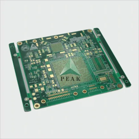
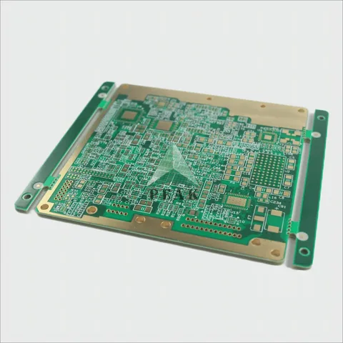
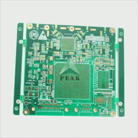
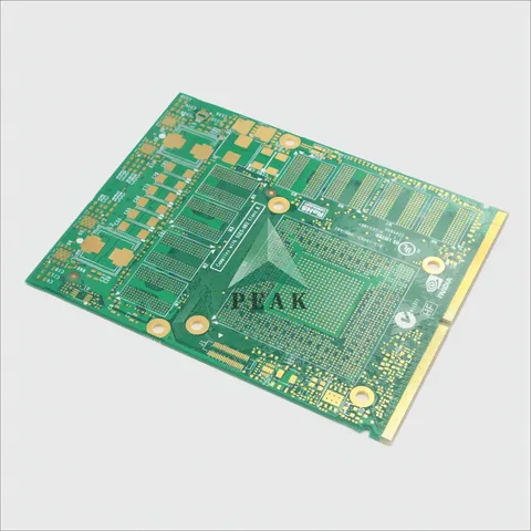
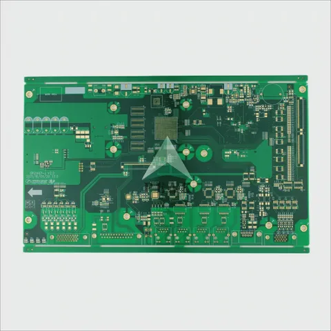
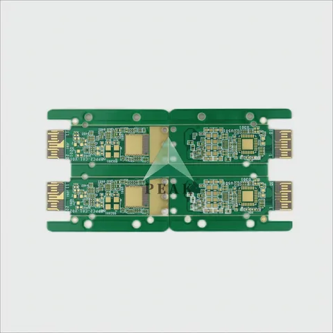
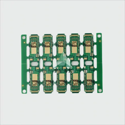
Multilayer PCB

14 Layers Rogers 4350B+FR4 TG170 Hybrid Lamination POFV ENIG Rigid PCB

Built as a 14-layer stack on Rogers 4350B+FR4 TG170, this board leaves the line at 2.0 mm thickness under ENIG 1u over green solder mask and white legend. The demanding part of this build is POFV processing, copper geometry held to 3.0 mil line width and 3.0 mil spacing, mechanical holes from 0.2 mm. The board is signed off to IPC-A-610 E Class II on outline by Rout / V-cut / Bridge / Stamp Hole and thickness to ±10%. Typical end use is electronic device.

  • Layers14 Layers (Max 64 Layers)
  • Base materialRogers 4350B+FR4 TG170
  • Finished thickness2.0 mm (Max 8mm)
  • Surface finishENIG 1u
  • Min. line width / spacing3.0 mil (Min 2mil) / 3.0 mil (Min 2mil)
  • Special processesPOFV

Quotation within 6 hours. Gerber, PowerPCB, CAD, AutoCAD, OrCAD, P-CAD, CAM-350 and CAM2000 files accepted.

What matters on this build

POFV

POFV runs on our own lines alongside POFV, backdrill, edge plating, plated half holes and step gold finger — no second supplier.

14-layer construction, scalable to 64 layers

This part is 14-layer; the same presses run 1 to 64 layers, so a stack-up revision does not force a supplier change.

Rogers 4350B+FR4 TG170 laminate

Built on Rogers 4350B+FR4 TG170 — RF laminate — drawn from over 120 laminate types held in the warehouse, from KB and ITEQ through Rogers, Isola and Panasonic.

3.0 mil / 3.0 mil line width and spacing

Etched to 3.0 mil width and 3.0 mil spacing here; the process floor is 2/2 mil inner at 1/3 oz copper, with ±10% accuracy on impedance layers.

ENIG 1u surface finish

Finished with ENIG 1u. ENIG 1–3 μin, ENEPIG, hard gold to 3.0 μm, immersion silver, immersion tin, OSP and lead-free HASL are all in-house.

Full specification as manufactured

These are the parameters this part was quoted, tooled and shipped against.

ParameterValue
PCB TypeHigh Frequency & Multilayer PCB
Number of Layers14 Layers (Max 64 Layers)
Finished Thickness2.0 mm (Max 8mm)
Base MaterialRogers 4350B+FR4 TG170
Copper Thickness1 oz
Min. Mechanical Hole0.2 mm (Min 0.1mm)
Min. Line Width3.0 mil (Min 2mil)
Min. Line Spacing3.0 mil (Min 2mil)
Surface FinishingENIG 1u
Solder MaskGreen
Silk ScreenWhite
Thickness Tolerance±10%
Impedance Control Accuracy±10% (min±5%)
Testing Service100% AOI ICT FCT Testing
Special ProcessesPOFV
PCB StandardIPC-A-610 E Class II
Brand NamePEAK PCB
Place of OriginShenzhen, Guangdong, China
Packaging InnerVacuum Packing/ Anti-Static Package
Packaging OuterExport Carton/ Customizable
PortShenzhen,Hongkong
Supply AbilitySample and Mass Production
Finished Inner Copper ThicknessHoz (Max 14oz)
Finished Outer Copper Thickness1oz (Max 14oz)
Outline ProfileRout/ V-cut/ Bridge/ Stamp Hole
ApplicationElectronic Device
Acceptable File FormatGerber file, Powerpcb, CAD, AUTOCAD, ORCAD, P-CAD, CAM-350, CAM2000

Questions engineers ask about this board

Can this design be scaled beyond 14 layers?

Yes. This part is quoted at 14 layers and the plant fabricates 1 to 64 layers, including sequential-lamination HDI up to 5+N(N+M)+5.

Can a different laminate be substituted for Rogers 4350B+FR4 TG170?

It can. Rogers 4350B+FR4 TG170 is what this part is built on, but material is a design input — Rogers, Arlon, Taconic, Isola, Nelco, Panasonic, TUC, ITEQ, SYTech, Ventec and KB grades are all stocked, and customer-supplied stock is accepted.

Is ENIG 1u the only surface finish offered on this board?

No. ENIG 1u is specified here; ENIG at 1–3 μin gold, ENEPIG, hard gold to 3.0 μm, immersion silver, immersion tin, OSP and lead-free HASL are alternatives, subject to panel size limits on HASL.

What files do you need to quote this part?

Gerber RS-274X plus a drill file and a stack-up or impedance note. PowerPCB, CAD, AutoCAD, OrCAD, P-CAD, CAM-350 and CAM2000 formats are also accepted. Quotation normally comes back within 6 hours.

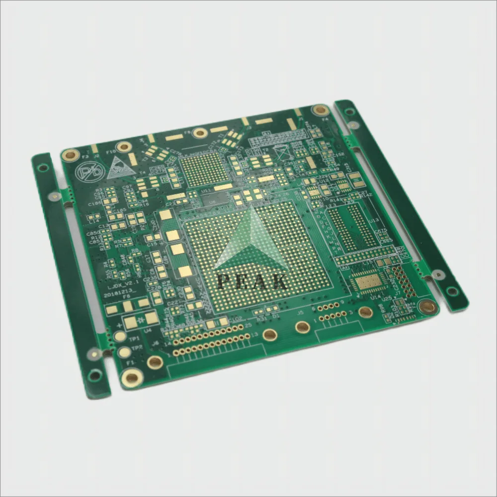
Other builds in Multilayer PCB

Get this board quoted

Send the part number or your own Gerber set. An engineer replies with price, lead time and any DFM comments — usually inside 6 hours.