PCB Assembly Process: A Detailed Walkthrough of the Manufacturing Process
Engineering reference · 1089 words · PEAK Technology
Assembly of printed circuit boards (PCBs) is an integral and vital aspect of electronics production, and this comprehensive guide seeks to walk you through each step of PCB assembly and its myriad techniques and processes involved.
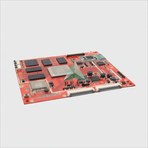
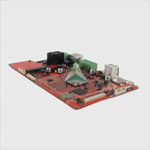
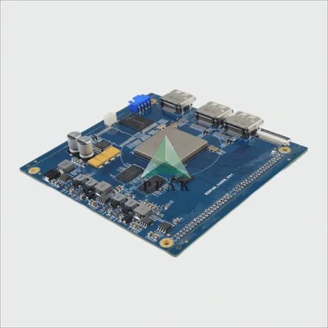
PCBA or printed circuit board assembly refers to the practice of mounting or placing electronic components onto a printed circuit board (PCB) to form an operational PCBA assembly, often via automated and manual techniques.
2. PCB Assembly Process: Component Acquisition
As with any journey, PCB assembly starts with preparation. For PCBs this involves purchasing all required components and PCBs – with this process relying heavily on your Bill of Materials (BOM) which lists every last resistor needed in your design.
Before assembly, solder paste should be evenly applied at every position where components will reside. This can be accomplished using a solder paste stencil designed based on your PCB design file.
4. PCB Assembly Process: Component Placement
Its Once components have been assembled on the PCB, they need to be placed. Automated machines known as Pick and Place machines are commonly employed for this task at high speed and precision.
5. PCB Assembly Process: Reflow Soldering
Once all components have been correctly assembled on the board, reflow soldering takes place. A PCB is heated in a reflow oven until all solder paste has melted away and formed an interconnection between component pins and PCB pads.
Some components do not lend themselves to surface mount technology (SMT) and must instead be soldered manually or through wave soldering.
7. PCB Assembly Process: Quality Inspection and Control
Once assembled, boards must undergo several checks post-assembly in order to ensure proper soldering quality and component placement. This may involve visual examination, Automated Optical Inspection (AOI), or X-ray inspection for BGAs and other hidden-solder devices.
8. PCB Assembly Process: Testing
Once assembled, PCB assemblies require rigorous testing in order to ensure correct functioning. Testing methods could include In-Circuit Test (ICT), Functional Circuit Test (FCT), or other board-specific assessments.
PCB Assembly Process: Conclusion
The PCB assembly process is intricate and precise at every step, serving as the link between electronics design and tangible, functioning devices. As electronics evolve and technologies get smaller and more sophisticated, exploring this intricate yet precise process is an engaging journey into how our electronic devices come to life.
What is PCB Assembly? PCB Assembly, often called PCBA, is the process of mounting electronic components onto a printed circuit board to make a functional PCB assembly.
What is the general process of PCB Assembly? The general steps in PCB assembly include applying solder paste to the board, placing the components, soldering them in place (often in an oven), inspection for quality assurance, and then testing the final assembly to ensure it functions as expected.
What’s the role of solder paste in the PCB Assembly process? Solder paste is a material used in the PCB assembly process. It’s a mix of flux and tiny grains of metal solder. It’s applied to the component pads on a PCB before placing components. Under heating in a reflow oven, it melts and forms a mechanical and electrical connection between the component and PCB.
What is a Pick and Place Machine? A pick and place machine is used in PCB assembly to place components onto the PCB quickly and accurately, it’s often used in automated assembly processes.
What is Reflow Soldering? Reflow soldering is a process that uses a continuous heat source to melt the solder paste after the components have been placed on the PCB. The PCB assembly is heated to a temperature that causes the solder paste to melt, or “reflow”, which solidifies to form a mechanical and electrical bond.
What is manual assembly, and when is it used? Manual assembly involves assembling the PCBs by hand, this process is typically used for low-volume or prototyping runs as it doesn’t necessarily require complicated machinery or setup.
What is automatic optical inspection (AOI)? AOI is a crucial step in PCB assembly used to quickly and accurately check for soldering defects, missing or incorrectly placed components, etc. It utilises cameras and software to perform inspections.
What is In-Circuit Testing (ICT)? ICT is a method of testing a PCB where a device known as a “Bed of Nails” tester makes contact to specific test points on the PCB, it’s often used to verify the correct function of components and the integrity of the PCB connections.
What is the Assembly Data required for PCB Assembly? The assembly data includes a Bill of Materials (BOM) detailing all the components to be placed on the board, PCB design files (Gerber files), Placement or Centroid data (includes X-Y component positions), and any special assembly instructions.