
Industry
Ceramic Substrates and Parts for Semiconductor and Electronics
Devices run hot because the isolating layer also blocks the thermal path
Where It Goes Wrong
- Devices run hot because the isolating layer also blocks the thermal path
- Substrate lots arrive out of flatness and jam automated assembly
- Small quantity substrate prototypes carry long lead times
What Buyers Ask For
- Substrates from 0.1 mm thick held to plus or minus 0.02 mm
- Laser scribing so panels snap cleanly into individual carriers
- A prototype quantity that does not require a production commitment
Parts We Supply Into Semiconductor and Electronics
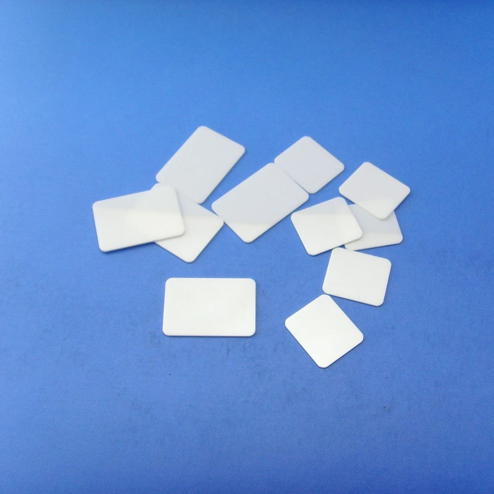
Al2O3 Alumina Ceramic PartsAl2O3 Alumina Ceramic SubstratesHeat spreading insulating plates from 0.1 mm thickness with laser scribingView specifications Metallized Ceramic PartsMetallized Alumina Ceramic RingMo Mn metallized and plated rings ready to braze to metalView specifications
 Al2O3 Alumina Ceramic Parts99% Al2O3 Alumina Ceramic Sheet Blank PlateSingle piece minimum order for wear plates and insulating blanksView specifications
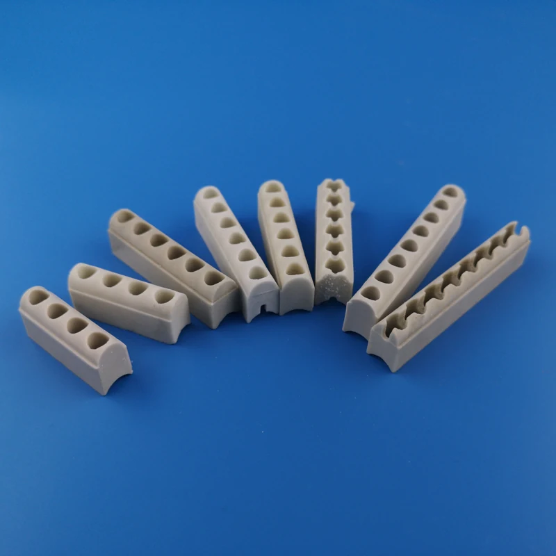 Steatite Ceramic PartsIndustrial Ceramic Insulator Heating Ring Ceramic StripOne to eight hole strips for flexible ceramic pad heatersView specifications
Typical Application Scenarios
Heat spreading plates under power electronics
Wafer processing and CVD or PVD coating heating stages
Hermetic feedthroughs and sealed housings
Insulating carriers in sensor and module assemblies
How a Part Gets Delivered
1. Drawing Review
Send a 2D or 3D drawing. We look at the features that drive cost: wall thickness, internal corners, ground versus as fired surfaces, and which dimensions are truly critical.
2. Material Selection
We propose a body from zirconia, alumina, steatite, silicon carbide or silicon nitride based on the temperature, the medium and whether the part takes impact.
3. Quotation
The quotation states the material, the achievable tolerances, the minimum order and the lead time before any tooling is committed.
4. Sample
Samples are delivered in 4 to 7 working days, free of charge with freight paid by the buyer.
5. Production
Forming, sintering, surface grinding, internal and external diameter grinding and precision CNC machining are all carried out in house.
6. Inspection and Shipping
Parts are inspected to your drawing with a report issued, and the packing and shipping process is photographed for your records.
Application Notes
Semiconductor and Electronics FAQ
How thin can the substrate be?
Minimum thickness is 0.1 mm, with a standard range of 0.1 mm to 2.0 mm.
How fast do substrates ship?
1 to 2 days for standard sizes in stock, 5 to 7 days for customized sizes.
Which substrate materials are available?
Alumina, zirconia, silicon nitride and aluminium nitride.
Tell Us What Is Failing
Send the part, the duty and the interval it currently survives. We come back with a material and a trial quantity.
Send a 2D or 3D drawing by WhatsApp or email. Samples in 4 to 7 working days.