
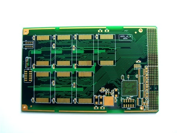
Four Layer Immersion Gold Board For Dense SMD Routing
A four layer FR4 board with an immersion nickel gold finish. The two inner layers are given over to a ground plane and a power plane, which frees both outer layers for routing and gives fine pitch devices a flat, planar surface to sit on.
What This Board Is
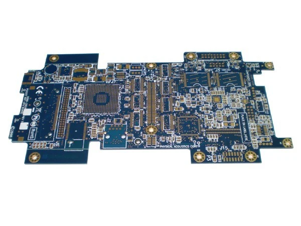
Adding two inner layers changes what a board can do. Return currents get a continuous ground plane instead of a meandering trace, supply rails stop dropping voltage across the board, and the outer layers are freed up for signal routing. The board shown carries an array of fine pitch connector footprints and a BGA site, both of which need the flat surface that immersion gold provides and neither of which places reliably on a HASL crown.
Inner layers are imaged, etched and AOI checked before the MLB laminator presses the stack-up.
- Rigid PCB
- 4 layer
- Immersion gold
- RoHS
What You Get From This Build
- Immersion gold is flat to within microns, so BGA and 0.4 mm pitch parts self-align during reflow
- A dedicated ground plane cuts radiated emissions without adding shielding cans to the assembly
- Gold over nickel does not oxidise, so boards can be stored and assembled in two separate batches
- Four layers carry roughly twice the routing density of a two layer board in the same outline
Who Specifies This Board
- Telecom equipment makers routing dense digital sections
- Industrial control OEMs whose boards must pass EMC testing
- Medical device manufacturers who need a stable, oxide-free finish for long storage
- Anyone placing a BGA, QFN or fine pitch connector for the first time
Four Failures This Build Is Designed Against
Each one is a real way this class of board goes wrong, and the tolerance or process decision that prevents it.
BGA balls that do not sit flat
Immersion gold gives a planar pad. There is no solder crown to tip the package, so the reflow self-alignment that BGA assembly depends on actually happens.
Radiated emissions failures late in the project
A continuous inner ground plane gives every high speed signal a short return path. Most emissions problems on two layer boards disappear when the same circuit moves to four layers.
Traces that will not fit in the outline
Minimum trace width and space are both 0.075 mm (3 mil), so escape routing from a fine pitch part fits without growing the board.
Oxidised pads after months in the warehouse
Gold does not oxidise. Boards can be built now and assembled later without a re-tinning step.
Technical Specification
Product detail from the catalogue record, followed by the published process capability for the Rigid PCB family. Anything the legacy catalogue did not record is marked TBC rather than filled in.
| Item | Technical specification |
|---|---|
| Product name | 4 Layer Rigid PCB |
| Legacy catalogue reference | 4 Layer |
| Product family | Rigid PCB |
| Layer count | 4 layer |
| Surface finish | Immersion gold |
| RoHS | RoHS compliant process, as recorded on the legacy catalogue |
| Layer count | 1 to 16 layers |
| Maximum panel dimension | 450 x 660 mm (18 x 26 in) |
| Minimum board thickness | 4 layers 0.40 mm (16 mil) / 6 layers 1.00 mm (40 mil) / 8 layers 1.20 mm (48 mil) |
| Minimum trace width | 0.075 mm (3 mil) |
| Minimum trace space | 0.075 mm (3 mil) |
| Minimum finished hole | 0.20 mm (8 mil) |
| Plated hole wall thickness | 0.025 mm (1 mil) |
| Plated hole diameter tolerance | ±0.075 mm (3 mil) |
| Non-plated hole diameter tolerance | ±0.05 mm (2 mil) |
| Hole position tolerance | ±0.05 mm (2 mil) |
| Outline dimension tolerance | ±0.10 mm (4 mil) |
| Minimum solder bridge | 0.10 mm (4 mil) |
| Warpage | ≤0.75% |
| Isolation resistance | >1012 Ω at normal condition |
| Hole resistance | <300 Ω at normal condition |
| Flammability rating | 94V-0 self-extinguishing |
| Open / short test voltage | 50 to 300 V |
What The Board Is Made Of
| Material | Specification |
|---|---|
| Base laminate | FR4 glass reinforced epoxy, 94V-0 self-extinguishing |
| Copper | Weight confirmed against the current your rails carry |
| Solder mask | LPI solder mask, green as standard, other colours on request |
| Legend | Silk screen legend ink, white as standard |
| Surface finish | Lead-free HASL, immersion nickel gold or electroplated nickel gold |
What Can Be Changed
- Layer count from 1 to 16
- Solder mask colour including blue and other colours
- Legend colour
- Lead-free HASL, immersion gold or electroplated gold
- Copper weight to suit the current your rails carry
- Delivery as singles, V-cut arrays or routed tab arrays
How This Board Is Made
Eight stages on equipment sourced from the USA, Japan, Germany and Israel. Every stage listed runs inside our own plant.
Film and tooling
Artwork plotted on a Mania 8850-P film plotter and the panel laid out for the order quantity.
Inner layers
Imaged, etched and checked before lamination, because a defect buried in the stack cannot be repaired.
Lamination
Cores and prepreg pressed on the MLB laminator to build the stack-up.
Drilling
Mania, Hitachi and domestic CNC drillers, thirteen machines in total, to a 0.20 mm minimum hole.
Plating
Desmear, automatic PTH line and graphic plating to a 0.025 mm barrel wall.
Mask and legend
Automatic screen printing and roller coating, then exposure and developing.
Surface finish
Lead-free HASL, immersion gold or electroplated gold according to the order.
Profile and test
CNC routing or V-cut to ±0.10 mm, then open and short testing at 50 to 300 V.
What Is Checked Before It Ships
- Inner layer inspection before lamination, because buried defects cannot be repaired
- Open and short testing at 50 to 300 V on every board
- Hole resistance verified below 300 Ω at normal condition
- Isolation resistance verified above 1012 Ω at normal condition
- Warpage held at ≤0.75% across the panel
What The Plant Holds
- ISO 9001:2000. Quality management system certification recorded by the company. Current revision year available on request.
- ISO 14001:1996. Environmental management system certification recorded by the company.
- UL. Certification recorded by the company. File number available on request.
- RoHS and lead free. Listed in the company environmental policy alongside pollution prevention and resource reduction.
Certificate numbers, issue dates and current revision years are not published on the legacy site. Ask for copies with your enquiry and they will be sent with the quotation.
How It Compares With The Alternatives
Three boards from our own catalogue, side by side, so the trade-off is visible rather than argued.
| Board | Layers or build | Finish | Best suited to |
|---|---|---|---|
| 4 Layer Rigid PCB | 4 | Immersion gold | Fine pitch SMD with ground and power planes |
| 2 Layer Rigid PCB | 2 | Lead-free HASL | Simpler circuits at lower cost |
| 6 Layer Rigid PCB | 6 | Lead-free HASL | More routing layers for larger controllers |
What To Send With Your Enquiry
Four things that decide whether the quote comes back right the first time.
- Send a stack-up drawing with the copper weight of each layer and the dielectric thickness between them.
- Mark which nets need controlled impedance and state the target value and tolerance.
- Keep BGA escape vias on the drill file rather than describing them in an email.
- Tell us if the board needs a gold thickness above our standard immersion deposit.
4 Layer Rigid PCB Questions
What is the minimum trace width and space you can hold?
0.075 mm, which is 3 mil, for both width and space. That figure is from our published rigid capacity table and applies to inner and outer layers.
Immersion gold or gold plating, which should I choose?
Immersion gold is flatter and better for fine pitch SMD. Electroplated gold is harder and better for contact surfaces such as edge fingers. Our 8 layer board uses gold plating for that reason.
Can you hold controlled impedance on four layers?
Send the target impedance and tolerance with your stack-up and we will confirm what the available laminate thicknesses allow before we tool the job.
How flat will the finished board be?
Warpage is held to 0.75% or better across the panel, which is the limit published in our rigid capacity table.
Other Boards In The Rigid PCB Family
Boards built on the same line, with the same tolerances, in a different configuration.
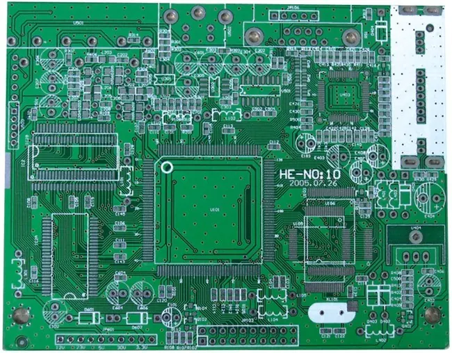
Double Sided FR4 Board With Lead Free HASL
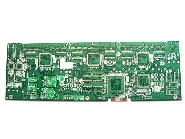
Six Layer Board With Lead Free HASL For Larger Controllers
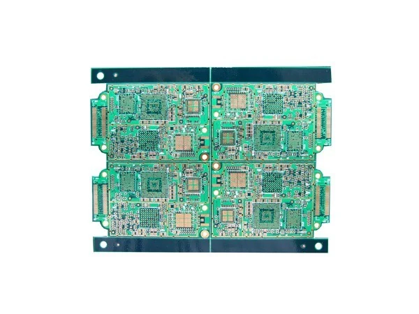
Eight Layer Board With Electroplated Gold For Contact Surfaces
Ten Layer Immersion Gold Board For High Density Digital Designs
Where This Board Is Used
The fields the legacy catalogue records for this class of board.
This Board In Context
Background Reading
Layer count is the single decision that most affects the price and the electrical behaviour of a board. This guide sets ...
Three surface finishes cover almost every board we build. Choosing between them is not a quality decision, it is a fitne...
Design rules are usually set once and copied between projects. That is fine until a board needs to shrink, at which poin...
Get 4 Layer Rigid PCB Priced Against Your Own Files
Send Gerber RS-274X with an NC drill file, or an ODB++ package, with the layer count, thickness, copper weight, surface finish and quantity. We check it against the published capability before quoting.