

Trace Width And Spacing And What They Cost You
Design rules are usually set once and copied between projects. That is fine until a board needs to shrink, at which point it matters exactly what the fabricator can hold and what it costs to ask for it. This guide explains the limits and the trade-offs behind them.
On This Page
What The Numbers Mean
Minimum trace width is the narrowest conductor the etching process will reliably produce across a whole panel. Minimum space is the smallest gap between two conductors that will still be fully cleared. Both are 0.075 mm, which is 3 mil, on our rigid line, for inner and outer layers alike.
Those are limits, not recommendations. A design that sits at the limit everywhere will yield worse than one that only approaches it where it has to, and yield is part of the price.
Where Tight Rules Actually Earn Their Cost
The places that genuinely need 3 mil rules are escape routing from fine pitch parts, and the fan-out under a BGA. Everywhere else, widening traces costs nothing and improves both yield and current capacity. A sensible layout uses wide traces by default and tightens only in the regions that demand it.
- BGA escape routing between pads
- Fan-out under fine pitch QFN and QFP devices
- Dense connector break-out on small boards
- Impedance controlled nets where the width is set by the stack-up
Spacing Is Also A Safety Question
On a board with mains or high voltage sections, spacing stops being a routing decision and becomes a creepage and clearance requirement set by whatever standard the product is built to. The process limit of 0.075 mm is irrelevant there. What matters is the clearance your standard requires, and that is a layout constraint you impose, not one we can infer.
The Other Limits That Travel With Them
| Parameter | Rigid FR4 | Aluminium | Flex |
|---|---|---|---|
| Minimum trace width | 0.075 mm | 0.15 mm | 0.05 mm |
| Minimum trace space | 0.075 mm | 0.15 mm | 0.05 mm |
| Minimum finished hole | 0.20 mm | 0.5 mm | 0.1 mm drilled |
| Minimum solder bridge | 0.10 mm | See specification | See specification |
| Hole position tolerance | ±0.05 mm | ±0.05 mm | See specification |
| Outline tolerance | ±0.10 mm | ±0.2 mm | ±0.05 mm |
Solder Mask Between Pads
Minimum solder bridge is 0.10 mm on the rigid line. Below that the strip of mask between two pads stops being reliable, and slivers of mask that come away during processing end up somewhere they should not be. If a fine pitch footprint needs mask between pads, check the pad gap against that figure before committing to the part.
Boards This Guide Applies To
Catalogue items where the decisions in this guide have already been made one way or another.
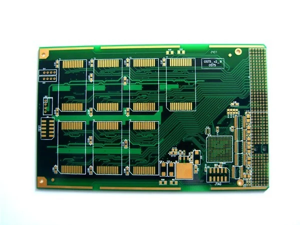
Four Layer Immersion Gold Board For Dense SMD Routing
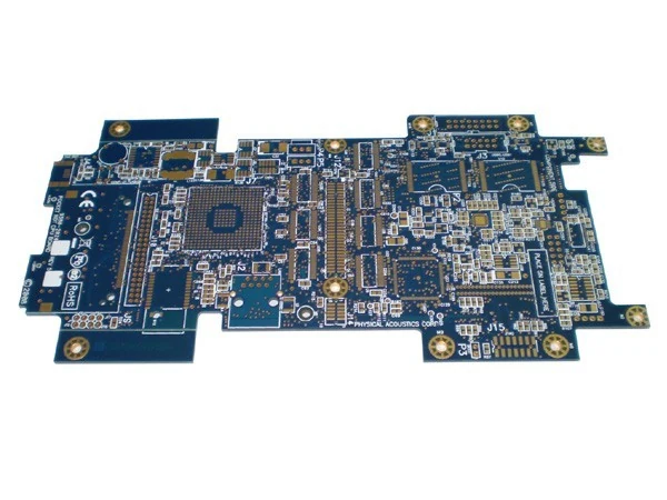
Ten Layer Immersion Gold Board For High Density Digital Designs
Assembled Compact Control Board With Connector Bank And Shielded Areas
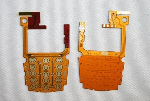
Double Layer Flex Circuit With Exposed Gold Contact Pads
Other Guides In The Knowledge Center
Eight guides in total, covering layer count, finishes, thermal management, flex design, tolerances and buying.
Layer count is the single decision that most affects the price and the electrical behaviour of a board. This guide sets ...

Three surface finishes cover almost every board we build. Choosing between them is not a quality decision, it is a fitne...
When a board runs hot the usual fixes are a bigger heatsink or a bigger enclosure. A metal core board attacks the proble...
Questions About This Topic
What is your minimum trace width and space?
0.075 mm, which is 3 mil, on both inner and outer layers of rigid FR4. Flex goes to 0.05 mm and aluminium is 0.15 mm.
Will a 3 mil design cost more than a 6 mil design?
Tighter rules affect yield, and yield affects price. Send both versions if you have them and we will quote them side by side.
Can you build boards with microvias?
Our published rigid process is a through-hole process with a 0.20 mm minimum hole. Send your via structure and we will tell you whether it fits.
Have A Board That This Guide Does Not Answer
Send the files and the question. We will tell you what the published capability allows and where your design sits against it.