
Ten Layer Immersion Gold Board For High Density Digital Designs
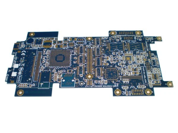
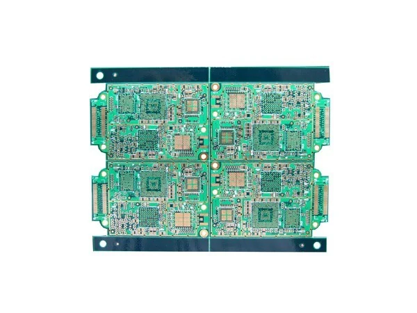
A ten layer FR4 board with immersion gold, built on a blue solder mask. Ten layers give six routing layers and four planes, which is the point at which several BGA devices can be escaped and routed on one board without pushing to blind vias.
What This Board Is
Once a design carries more than one large BGA, the escape routing alone consumes two layers. Ten layers give that back. The board photographed uses a blue mask over a dense multi-device layout with several plane splits, and the immersion gold finish keeps every fine pitch pad flat for placement.
Multiple inner cores are laminated in sequence, then drilled on Hitachi and Mania CNC drillers before PTH.
- Rigid PCB
- 10 layer
- Immersion gold
- RoHS
What You Get From This Build
- Six routing layers escape multiple BGA devices without resorting to blind or buried vias
- Four plane layers allow separate supply voltages to have their own copper
- Immersion gold keeps hundreds of fine pitch pads coplanar for reliable first-pass assembly
- Solder mask colour is selectable, and the board shown uses blue rather than the default green
Who Specifies This Board
- Telecom and networking equipment builders with multi-BGA designs
- Computing hardware makers building embedded modules
- Industrial vision and motion control OEMs running high speed buses
- Design houses prototyping a board that will later run in volume
Four Failures This Build Is Designed Against
Each one is a real way this class of board goes wrong, and the tolerance or process decision that prevents it.
Not enough layers to break out a large BGA
Each BGA row needs its own routing channel. Ten layers give the channel count that lets escape routing finish without blind vias, which are far more expensive.
Three or four supply voltages fighting for one plane
Four plane layers mean each rail can have continuous copper rather than a split that creates return path discontinuities.
Barrel cracking in a thick stack
Plated hole wall thickness is held at 0.025 mm through the full stack depth, and hole resistance is verified below 300 ohms.
Leakage between closely spaced planes
Isolation resistance is held above 10 to the power 12 ohms at normal condition.
Technical Specification
Product detail from the catalogue record, followed by the published process capability for the Rigid PCB family. Anything the legacy catalogue did not record is marked TBC rather than filled in.
| Item | Technical specification |
|---|---|
| Product name | 10 Layer Rigid PCB |
| Legacy catalogue reference | 10 Layer |
| Product family | Rigid PCB |
| Layer count | 10 layer |
| Surface finish | Immersion gold |
| RoHS | RoHS compliant process, as recorded on the legacy catalogue |
| Layer count | 1 to 16 layers |
| Maximum panel dimension | 450 x 660 mm (18 x 26 in) |
| Minimum board thickness | 4 layers 0.40 mm (16 mil) / 6 layers 1.00 mm (40 mil) / 8 layers 1.20 mm (48 mil) |
| Minimum trace width | 0.075 mm (3 mil) |
| Minimum trace space | 0.075 mm (3 mil) |
| Minimum finished hole | 0.20 mm (8 mil) |
| Plated hole wall thickness | 0.025 mm (1 mil) |
| Plated hole diameter tolerance | ±0.075 mm (3 mil) |
| Non-plated hole diameter tolerance | ±0.05 mm (2 mil) |
| Hole position tolerance | ±0.05 mm (2 mil) |
| Outline dimension tolerance | ±0.10 mm (4 mil) |
| Minimum solder bridge | 0.10 mm (4 mil) |
| Warpage | ≤0.75% |
| Isolation resistance | >1012 Ω at normal condition |
| Hole resistance | <300 Ω at normal condition |
| Flammability rating | 94V-0 self-extinguishing |
| Open / short test voltage | 50 to 300 V |
What The Board Is Made Of
| Material | Specification |
|---|---|
| Base laminate | FR4 glass reinforced epoxy, 94V-0 self-extinguishing |
| Copper | Weight confirmed against the current your rails carry |
| Solder mask | LPI solder mask, green as standard, other colours on request |
| Legend | Silk screen legend ink, white as standard |
| Surface finish | Lead-free HASL, immersion nickel gold or electroplated nickel gold |
What Can Be Changed
- Layer count from 1 to 16
- Solder mask colour including blue and other colours
- Legend colour
- Lead-free HASL, immersion gold or electroplated gold
- Copper weight to suit the current your rails carry
- Delivery as singles, V-cut arrays or routed tab arrays
How This Board Is Made
Eight stages on equipment sourced from the USA, Japan, Germany and Israel. Every stage listed runs inside our own plant.
Film and tooling
Artwork plotted on a Mania 8850-P film plotter and the panel laid out for the order quantity.
Inner layers
Imaged, etched and checked before lamination, because a defect buried in the stack cannot be repaired.
Lamination
Cores and prepreg pressed on the MLB laminator to build the stack-up.
Drilling
Mania, Hitachi and domestic CNC drillers, thirteen machines in total, to a 0.20 mm minimum hole.
Plating
Desmear, automatic PTH line and graphic plating to a 0.025 mm barrel wall.
Mask and legend
Automatic screen printing and roller coating, then exposure and developing.
Surface finish
Lead-free HASL, immersion gold or electroplated gold according to the order.
Profile and test
CNC routing or V-cut to ±0.10 mm, then open and short testing at 50 to 300 V.
What Is Checked Before It Ships
- Inner layer inspection before lamination, because buried defects cannot be repaired
- Open and short testing at 50 to 300 V on every board
- Hole resistance verified below 300 Ω at normal condition
- Isolation resistance verified above 1012 Ω at normal condition
- Warpage held at ≤0.75% across the panel
What The Plant Holds
- ISO 9001:2000. Quality management system certification recorded by the company. Current revision year available on request.
- ISO 14001:1996. Environmental management system certification recorded by the company.
- UL. Certification recorded by the company. File number available on request.
- RoHS and lead free. Listed in the company environmental policy alongside pollution prevention and resource reduction.
Certificate numbers, issue dates and current revision years are not published on the legacy site. Ask for copies with your enquiry and they will be sent with the quotation.
How It Compares With The Alternatives
Three boards from our own catalogue, side by side, so the trade-off is visible rather than argued.
| Board | Layers or build | Finish | Best suited to |
|---|---|---|---|
| 10 Layer Rigid PCB | 10 | Immersion gold | Multi-BGA high density digital boards |
| 12 Layer Rigid PCB | 12 | Immersion gold | Backplanes and the densest routing |
| 6 Layer Rigid PCB | 6 | Lead-free HASL | Mid density boards without fine pitch parts |
What To Send With Your Enquiry
Four things that decide whether the quote comes back right the first time.
- Provide a full stack-up drawing. On a ten layer board the layer order is not something to leave open.
- Mark controlled impedance nets with target values and tolerances per layer.
- State the solder mask colour explicitly if you want blue rather than green.
- Flag any aspect ratio above 8:1 so we can confirm the drill and plating route before quoting.
10 Layer Rigid PCB Questions
How many layers can you build in total?
Our rigid capacity table covers 1 to 16 layers. Ten and twelve layer boards are in regular production.
Can I have a blue or black solder mask?
Yes. The board shown here uses blue. Tell us the colour with the order and we will confirm it before tooling.
What is the smallest hole you can drill and plate?
0.20 mm finished, which is 8 mil, as published in our rigid capacity table.
Do you check hole resistance on multilayer boards?
Hole resistance is verified below 300 ohms at normal condition, alongside open and short testing at 50 to 300 V.
Other Boards In The Rigid PCB Family
Boards built on the same line, with the same tolerances, in a different configuration.
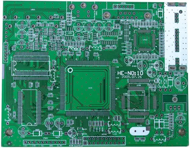
Double Sided FR4 Board With Lead Free HASL
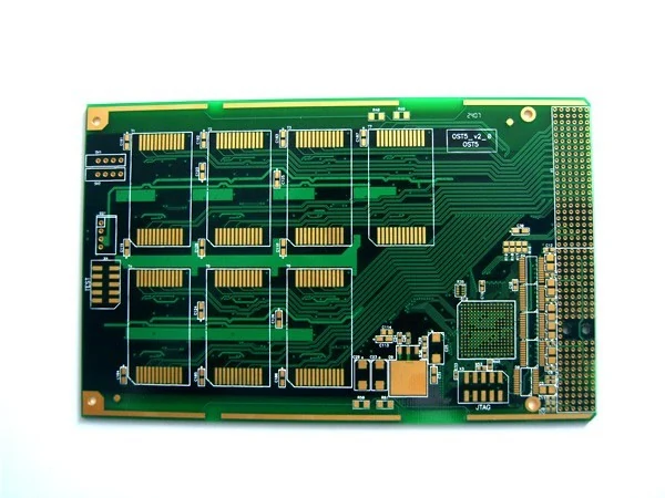
Four Layer Immersion Gold Board For Dense SMD Routing
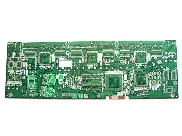
Six Layer Board With Lead Free HASL For Larger Controllers
Eight Layer Board With Electroplated Gold For Contact Surfaces
Where This Board Is Used
The fields the legacy catalogue records for this class of board.
This Board In Context
Background Reading
Layer count is the single decision that most affects the price and the electrical behaviour of a board. This guide sets ...
Design rules are usually set once and copied between projects. That is fine until a board needs to shrink, at which poin...
Get 10 Layer Rigid PCB Priced Against Your Own Files
Send Gerber RS-274X with an NC drill file, or an ODB++ package, with the layer count, thickness, copper weight, surface finish and quantity. We check it against the published capability before quoting.