
Flexible Circuits That Replace Harnesses And Flat Cables
Single layer, double layer and multilayer flexible circuits on PI, PET and FR4, up to 406 x 610 mm, with 0.05 mm track and gap, 0.1 mm drilled holes and an outline tolerance of ±0.05 mm from V-cut, punch, mill or laser.
Every Flex PCB Board In The Catalogue
Each board below is a catalogue item with its own photograph, layer count and recorded surface finish.
What This Family Is For
A wiring harness is the least repeatable part in most assemblies. Conductors sit slightly differently on every unit, splices fail, and the part takes hand labour that cannot be inspected properly. A flexible circuit is etched, so every conductor is in the same place on every unit, and the shape can follow the mechanism instead of being forced into it. Our flex line runs four different outline processes because the right one depends on the shape.
Who Buys Flex PCB From Us
- Camera, optical and imaging module manufacturers
- Display and panel integrators connecting boards in different planes
- Membrane keypad and control panel builders
- Medical instrument makers routing signals through moving joints
Typical Applications
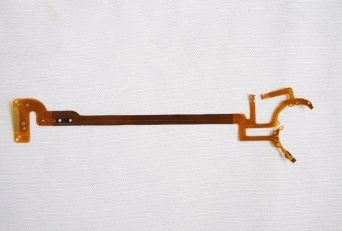
- Branched circuits replacing a multi-wire harness inside a mechanism
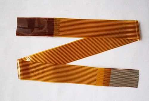
- Board to board ribbons with stiffened ZIF tails at both ends
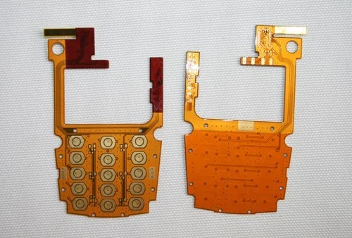
- Membrane keypad circuits with plated or carbon contact pads
- Flex tails on assemblies where a connector would be a failure point
Four Reasons This Family Is Built Here
Each point below is backed by a figure from the published capability tables rather than by a claim.
- 0.05 mm track and gap. Two mil width and gap, which is what fits a high conductor count into a narrow ribbon.
- Four outline processes. Precise V-cut, punching, milling and laser outline, all held to ±0.05 mm, so the process suits the shape rather than the shape suiting the process.
- Copper from 9 to 70 µm. The same ribbon format can carry signal or supply current depending on the base copper chosen.
- Full ink and coverlay range. PI and PET coverlay, LPI and UV-cured soldermask, legend ink, peelable mask, carbon ink and silver paste for contact areas.
Flexible PCB Capacity
These are the figures the plant builds to. Check your design against them before ordering rather than after the first article.
| Item | Technical specification |
|---|---|
| Layer count | Single layer, double layer and multilayer |
| Base material | PI, FR4, PET |
| Base copper thickness | 9, 12, 18, 35 and 70 µm |
| Maximum board size | 406 x 610 mm (16 x 24 in) |
| Minimum hole, drilled | φ0.1 mm (0.004 in) |
| Minimum hole, punched | φ0.5 mm (0.02 in) |
| Plated hole tolerance | ±0.05 mm (±0.002 in) |
| Minimum track width | 0.05 mm (2 mil) |
| Minimum track gap | 0.05 mm (2 mil) |
| Surface treatment | Plated or immersion tin, plated or immersion gold, OSP |
| Outline treatment | Precise V-cut, punch, milled, laser outline |
| Outline tolerance | ±0.05 mm |
| Coverlay | PI film and PET film lamination |
| Solder resist inks | LPI soldermask, UV-cured soldermask, legend ink, peelable soldermask, carbon ink, silver paste |
| Peeling strength | 1.0 kgf/cm with adhesive copper, 0.5 kgf/cm with adhesiveless copper |
| Legend colours | Multiple silk-screen colours |
Flex PCB Boards In Use
Boards from this family and the problem each one had to solve. Customer names and volumes are confidential.
Where Flex PCB Boards End Up
The industries the legacy catalogue records for this board family.
Guides Related To Flex PCB
Written for buyers and designers working with this board family.
Flex PCB Questions
Which base material should I use?
Polyimide where the part is soldered or flexes repeatedly, PET for low cost static applications, and FR4 where a rigid island is needed within the part.
What is the smallest track you can etch on flex?
0.05 mm track and 0.05 mm gap, which is 2 mil for both.
How do you cut the outline?
Precise V-cut, punching, milling or laser outline, held to ±0.05 mm. The choice depends on the shape and the volume.
What surface finishes are available on flex?
Plated or immersion tin, plated or immersion gold, and OSP.
Can you print carbon or silver on contact pads?
Yes. Carbon ink and silver paste are both part of our flex process.
Get A Flex PCB Quote From The Plant That Builds Them
Send your Gerber or ODB++ package with the layer count, thickness, copper weight, surface finish and quantity. We check it against the capability table above before quoting.