
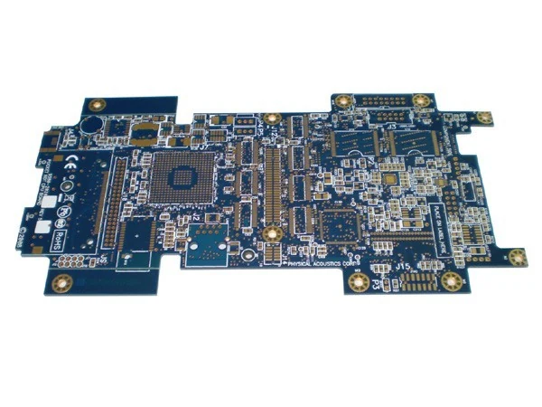
Dense Digital Boards With Controlled Return Paths
Telecom boards are dense, they run fast, and they have to pass emissions testing. That combination pushes layer count up and design rules down. Our rigid line runs to 16 layers with 0.075 mm trace and space, which is the envelope most of this work sits inside.
What Actually Fails In Telecommunication
Four failure modes specific to this sector, and the published figure that each one is controlled by.
Emissions
A continuous inner ground plane gives every fast signal a short return path, which fixes most emissions problems before they reach the test house.
Escape routing
Multi-BGA designs consume routing layers just getting out of the package. Ten and twelve layer builds give those layers back.
Slot fit
Line cards go into a fixed slot pitch. Outline tolerance of ±0.10 mm and hole position of ±0.05 mm keep the card in its guides.
Connector wear
Cards that are re-seated during maintenance need electroplated gold, not immersion.
Boards We Build For This Sector
Telecom work is mostly eight to twelve layer rigid with immersion gold, with electroplated gold where edge fingers are mated repeatedly. Send the impedance profile with the stack-up.
Ten Layer Immersion Gold Board For High Density Digital Designs
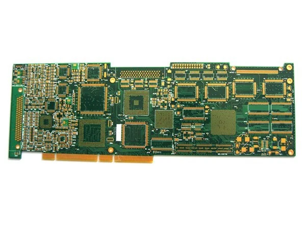
Twelve Layer Immersion Gold Board With Edge Connector Fingers
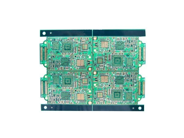
Eight Layer Board With Electroplated Gold For Contact Surfaces
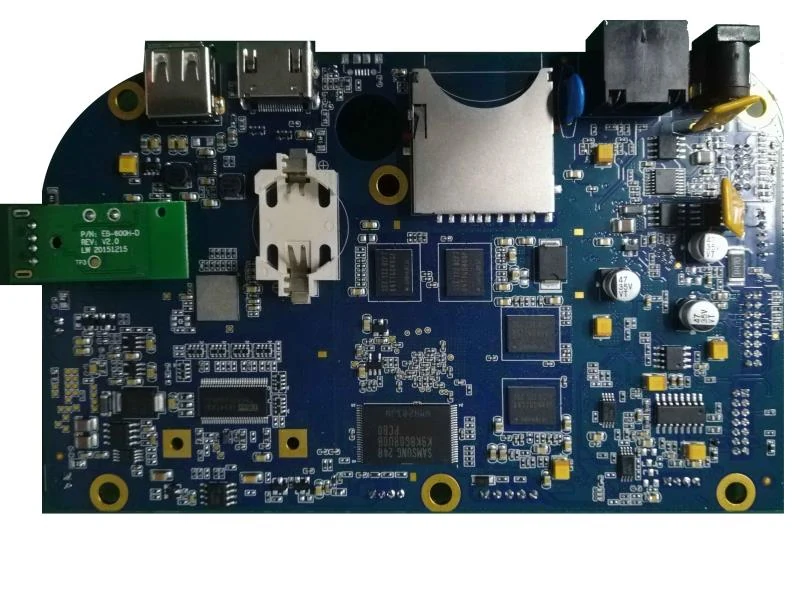
Assembled Multi Port Board With USB Card Slot And Shielded Modules
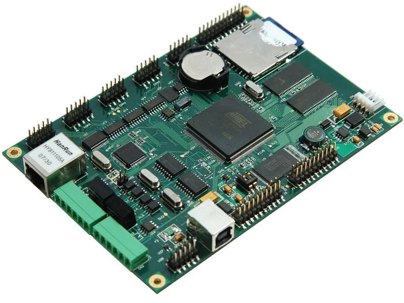
Assembled Embedded Controller With Microcontroller Ethernet And Storage
Four Ways To Buy For A Telecommunication Programme
Prototyping, design support, turnkey assembly and one stop supply across all three substrate families.
Fast Turn Prototyping
Get The First Boards Back Before The Design Goes Cold
SolutionPCB Design Support
Design Review Against Real Process Limits
SolutionTurnkey PCBA Assembly
Bare Board And Assembly Quoted As One Finished Unit
SolutionOne Stop Supply
One Supplier For Rigid Aluminium Flex And Assembly
An Example From This Sector
Boards from the production catalogue and the problem each had to solve. Customer names and volumes are confidential.
Guides For Telecommunication Buyers
Written for the engineering and purchasing decisions this sector runs into.
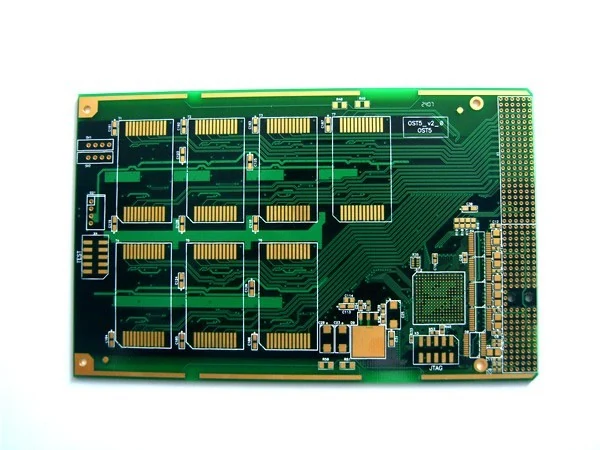
Layer count is the single decision that most affects the price and the electrical behaviour of a board. This guide sets ...
Three surface finishes cover almost every board we build. Choosing between them is not a quality decision, it is a fitne...

Design rules are usually set once and copied between projects. That is fine until a board needs to shrink, at which poin...
Telecommunication Questions
Can you hold controlled impedance?
Send the target impedance and tolerance per net with your stack-up and we will confirm it against available laminate thicknesses before tooling.
What is your highest layer count?
16 layers is the published limit on our rigid capacity table.
Do you build backplanes?
Twelve layer boards with edge connectors are in the catalogue and are the usual backplane construction.
Send Us A Telecommunication Board To Price
Gerber or ODB++ with the layer count, thickness, copper weight, surface finish and quantity. Add the bill of materials if you want the board assembled as well.