
A Practical Design Guide For Flexible Circuits
Flexible circuits fail in ways rigid boards do not: creases in the wrong place, copper fatigue at a fold, tails that buckle in a connector. Most of it is designed in rather than manufactured in. This guide covers the decisions that matter.
On This Page
Decide Where The Part Bends Before You Route It
A flexible circuit is not uniformly flexible. Coverlay, stiffeners and copper density all change how a region behaves. The first thing to establish is which areas are free to bend, which are held rigid, and how many times each bend happens: once at assembly, or repeatedly in service.
A one-time installation fold and a fold that cycles a million times are different engineering problems. The first needs a sensible radius. The second needs the copper routed along the neutral axis and usually a thinner base copper.
Copper Thickness Is A Mechanical Choice
Base copper is available from 9 to 70 micrometres. Thicker copper carries more current and fatigues faster at a fold. On a part that flexes in service, choose the thinnest copper that carries the current, and run traces perpendicular to the bend axis wherever the layout allows.
Stiffeners Are Not Optional On Connector Tails
A bare flex tail entering a ZIF connector will buckle. A stiffener laminated underneath the contact area gives the tail the thickness the connector expects and lets it grip properly. Specify the stiffener material and thickness on the drawing, and mark the area it covers, because the connector datasheet gives a total insertion thickness that has to be met.
- Mark stiffener areas on their own layer
- Give the stiffener material and thickness explicitly
- Check the total tail thickness against the connector datasheet
- Remember that both ends of a ribbon usually need one
Coverlay And Openings
Coverlay is a laminated film, not a printed mask, so its openings are cut before lamination and have their own tolerance. Keep the openings on a separate layer from any solder mask layer in your output, because the two are different processes and will be read by different people.
On keypad and contact circuits the openings expose the pads that are touched. Those pads then need a contact finish: plated or immersion gold for signal contacts, carbon ink or silver paste where the switch mechanism allows it.
Outline Processes
There are four ways to cut a flex outline and they are not interchangeable. Precise V-cut suits straight break lines in an array. Punching is fast and repeatable for volume with a simple shape. Milling handles one-off and low volume shapes. Laser outline handles fine detail and tight internal radii that a punch cannot reach. All four are held to ±0.05 mm.
| Parameter | Capability |
|---|---|
| Base material | PI, FR4, PET |
| Base copper | 9, 12, 18, 35, 70 µm |
| Minimum track and gap | 0.05 mm (2 mil) |
| Minimum hole, drilled | φ0.1 mm |
| Minimum hole, punched | φ0.5 mm |
| Maximum board size | 406 x 610 mm |
| Outline tolerance | ±0.05 mm |
| Peeling strength | 1.0 kgf/cm adhesive, 0.5 kgf/cm adhesiveless |
Boards This Guide Applies To
Catalogue items where the decisions in this guide have already been made one way or another.
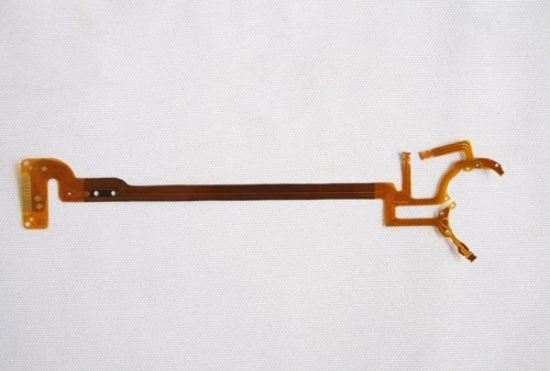
Single Layer Flex Circuit With Branched Arms And ZIF Tail
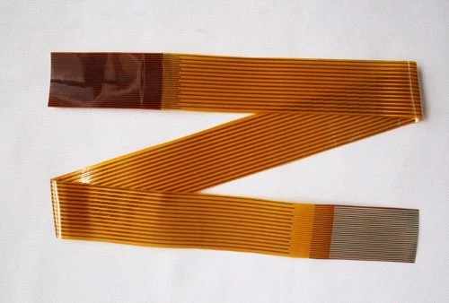
Single Layer Flex Ribbon With Parallel Conductors And End Stiffeners
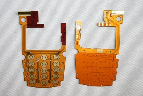
Double Layer Flex Circuit With Exposed Gold Contact Pads
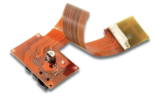
Assembled Rigid Flex Unit Linking A Connector Board To A Flex Tail
Other Guides In The Knowledge Center
Eight guides in total, covering layer count, finishes, thermal management, flex design, tolerances and buying.
Layer count is the single decision that most affects the price and the electrical behaviour of a board. This guide sets ...
Three surface finishes cover almost every board we build. Choosing between them is not a quality decision, it is a fitne...
When a board runs hot the usual fixes are a bigger heatsink or a bigger enclosure. A metal core board attacks the proble...
Questions About This Topic
What bend radius should I use?
It depends on copper thickness, coverlay and whether the bend cycles. Send the installed bend radius with the flat pattern and we will check it against the copper you have chosen.
Can you laminate stiffeners in more than one place?
Yes. Mark each stiffener area separately with its material and thickness.
Do you supply flexible circuits already assembled?
Yes. Flex assembly is part of our PCBA range and uses carriers that hold the part flat through reflow.
Have A Board That This Guide Does Not Answer
Send the files and the question. We will tell you what the published capability allows and where your design sits against it.