
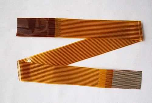
Single Layer Flex Ribbon With Parallel Conductors And End Stiffeners
A single layer polyimide ribbon carrying many parallel conductors, stiffened at both ends and folded into a Z to show its flexibility. This is the format used to connect two boards that move relative to each other, or that sit in different planes inside one housing.
What This Board Is
Where the branched flex circuit replaces a harness, this ribbon replaces a flat cable assembly. Every conductor is etched at the same pitch along the full length, and both ends carry a stiffener so they seat properly in their connectors. The Z fold in the photograph is how the part actually installs: it takes up slack without putting a sharp crease in the copper.
Ribbons are etched from roll stock, coverlay laminated, then punched to the flat pattern.
- Flex PCB
- 1 layer
- See specification
What You Get From This Build
- Uniform conductor pitch over the whole length removes the crosstalk variation of a twisted bundle
- Stiffeners at both ends give two reliable ZIF or LIF insertions from one part
- Base copper is available from 9 to 70 µm, so the ribbon can carry signal or power
- Folded installation absorbs mechanical tolerance between two boards without strain on either connector
Who Specifies This Board
- Display and panel module integrators
- Instrument makers connecting a front panel board to a main board
- Equipment builders with hinged or sliding assemblies
- Manufacturers standardising on one ribbon instead of several cable part numbers
Four Failures This Build Is Designed Against
Each one is a real way this class of board goes wrong, and the tolerance or process decision that prevents it.
Flat cables that snag or get pinched on assembly
A flex ribbon folds to a known shape and stays there. It does not wander inside the housing the way a loose cable does.
Ribbon ends that fray or delaminate at the contact
End stiffeners hold the contact area rigid, so repeated insertion does not damage the conductors.
A signal ribbon asked to carry supply current
Base copper thickness is selectable up to 70 µm, which lets one ribbon carry both signal and power.
Ribbons that are slightly too short in the assembly
Outline tolerance is ±0.05 mm, so length is repeatable across the whole batch.
Technical Specification
Product detail from the catalogue record, followed by the published process capability for the Flex PCB family. Anything the legacy catalogue did not record is marked TBC rather than filled in.
| Item | Technical specification |
|---|---|
| Product name | 1 Layer Flex Ribbon Cable |
| Legacy catalogue reference | 1 Layer(FPC) |
| Product family | Flex PCB |
| Layer count | 1 layer |
| Surface finish | See specification |
| Layer count | Single layer, double layer and multilayer |
| Base material | PI, FR4, PET |
| Base copper thickness | 9, 12, 18, 35 and 70 µm |
| Maximum board size | 406 x 610 mm (16 x 24 in) |
| Minimum hole, drilled | φ0.1 mm (0.004 in) |
| Minimum hole, punched | φ0.5 mm (0.02 in) |
| Plated hole tolerance | ±0.05 mm (±0.002 in) |
| Minimum track width | 0.05 mm (2 mil) |
| Minimum track gap | 0.05 mm (2 mil) |
| Surface treatment | Plated or immersion tin, plated or immersion gold, OSP |
| Outline treatment | Precise V-cut, punch, milled, laser outline |
| Outline tolerance | ±0.05 mm |
| Coverlay | PI film and PET film lamination |
| Solder resist inks | LPI soldermask, UV-cured soldermask, legend ink, peelable soldermask, carbon ink, silver paste |
| Peeling strength | 1.0 kgf/cm with adhesive copper, 0.5 kgf/cm with adhesiveless copper |
| Legend colours | Multiple silk-screen colours |
What The Board Is Made Of
| Material | Specification |
|---|---|
| Base material | PI, PET or FR4 |
| Base copper | 9, 12, 18, 35 or 70 µm |
| Coverlay | PI film or PET film lamination |
| Solder resist | LPI, UV-cured, peelable mask, legend ink, carbon ink or silver paste |
| Adhesion | 1.0 kgf/cm with adhesive copper, 0.5 kgf/cm adhesiveless |
What Can Be Changed
- PI, PET or FR4 base material
- Base copper from 9 to 70 µm
- Stiffeners in any number of positions
- Plated or immersion tin, gold, or OSP
- Carbon ink and silver paste contact printing
- V-cut, punch, mill or laser outline
How This Board Is Made
Eight stages on equipment sourced from the USA, Japan, Germany and Israel. Every stage listed runs inside our own plant.
Material selection
PI, PET or FR4 base chosen against whether the part is soldered and how often it flexes.
Imaging and etching
Circuit etched to a 0.05 mm minimum track and gap.
Coverlay
PI or PET film laminated over the conductors with openings cut at the contact areas.
Stiffeners
Laminated where connector tails or component areas need to be held rigid.
Hole forming
Drilled to φ0.1 mm or punched to φ0.5 mm depending on the feature.
Surface finish
Plated or immersion tin, plated or immersion gold, or OSP.
Contact printing
Carbon ink or silver paste printed where a contact pad needs it.
Outline
Precise V-cut, punch, mill or laser to ±0.05 mm.
What Is Checked Before It Ships
- Peeling strength of 1.0 kgf/cm on adhesive copper and 0.5 kgf/cm on adhesiveless copper
- Outline tolerance verified at ±0.05 mm after punching or laser cutting
- Coverlay opening registration checked against the contact areas
- Plated hole tolerance held at ±0.05 mm
- Stiffener thickness checked against the connector insertion specification
What The Plant Holds
- ISO 9001:2000. Quality management system certification recorded by the company. Current revision year available on request.
- ISO 14001:1996. Environmental management system certification recorded by the company.
- UL. Certification recorded by the company. File number available on request.
- RoHS and lead free. Listed in the company environmental policy alongside pollution prevention and resource reduction.
Certificate numbers, issue dates and current revision years are not published on the legacy site. Ask for copies with your enquiry and they will be sent with the quotation.
How It Compares With The Alternatives
Three boards from our own catalogue, side by side, so the trade-off is visible rather than argued.
| Board | Layers or build | Finish | Best suited to |
|---|---|---|---|
| 1 Layer Flex Ribbon Cable | 1 | See specification | Board to board ribbon interconnects |
| 1 Layer Flexible PCB | 1 | See specification | Shaped and branched harness replacements |
| 2 Layer Flexible PCB | 2 | See specification | Flex circuits with exposed contact pads |
What To Send With Your Enquiry
Four things that decide whether the quote comes back right the first time.
- Give the conductor count, the pitch and the exposed contact length at each end.
- State the contact side at each end. Ribbons are often specified with opposite side contacts.
- Mark the stiffener area and thickness for each end separately.
- Give the installed fold positions so we can check the bend radius against the copper thickness.
1 Layer Flex Ribbon Cable Questions
What copper thicknesses can I choose?
9, 12, 18, 35 and 70 micrometres, from our published flex capacity table.
How wide can a flex ribbon be?
Maximum board size on our flex line is 406 x 610 mm, which is 16 x 24 inches.
Can the contacts be on opposite sides at each end?
Yes, that is a common requirement. Mark the contact side clearly at both ends of the drawing.
What coverlay do you use?
PI film or PET film lamination. Polyimide is the default where the part is soldered.
Other Boards In The Flex PCB Family
Boards built on the same line, with the same tolerances, in a different configuration.
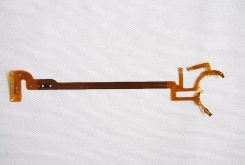
Single Layer Flex Circuit With Branched Arms And ZIF Tail
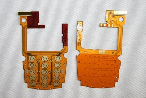
Double Layer Flex Circuit With Exposed Gold Contact Pads
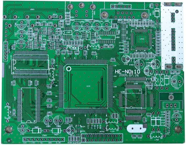
Double Sided FR4 Board With Lead Free HASL
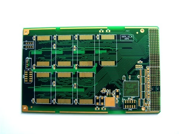
Four Layer Immersion Gold Board For Dense SMD Routing
Where This Board Is Used
The fields the legacy catalogue records for this class of board.
This Board In Context
Get 1 Layer Flex Ribbon Cable Priced Against Your Own Files
Send Gerber RS-274X with an NC drill file, or an ODB++ package, with the layer count, thickness, copper weight, surface finish and quantity. We check it against the published capability before quoting.