
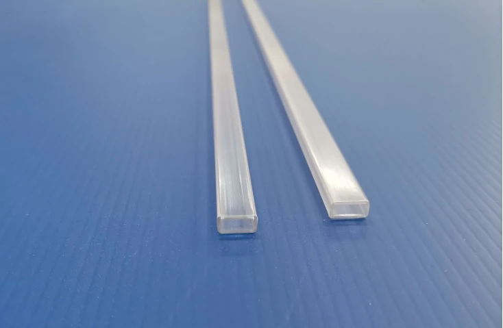
ESD Packaging For Semiconductor And IC Distribution
IC distributors and semiconductor plants handle devices that are sensitive to electrostatic discharge, mechanical shock, and orientation changes during transit.
- Home
- Industries
- Semiconductor And IC Distribution
IC distributors and semiconductor plants handle devices that are sensitive to electrostatic discharge, mechanical shock, and orientation changes during transit. SEWATE supplies anti-static packaging in the form of tubes, carrier tape, and reels, designed to maintain fixed orientation and ESD protection from the die house to the pick and place machine. Profiles are matched to DIP, SOIC, SOJ, PLCC, LCC, SOP, SSOP, TSSOP, QFN, MLF, LPCC, TO series, and sockets, with over a thousand open tools available for through-hole, SMT, and leadless packages.
What Goes Wrong in Semiconductor And IC Distribution
Devices arrive in random orientation, requiring manual sorting before assembly
Tube profiles that do not match the device body cause jams and shingling in high-speed feeders
Electrostatic discharge damage is detected only at incoming inspection, leading to rejected batches
Partial reels or tubes without traceable packaging complicate inventory and rework
Newly released packages lack available stock tube or tape profiles in standard catalogues
What Semiconductor And IC Distribution Buyers Need From Packaging
- Fixed orientation packaging that loads reliably into tube and tape feeders without manual intervention
- Consistent anti-static performance that does not degrade after handling or storage
- Tolerance control tight enough to support high-speed automated loading on fine-pitch and small body devices
- Repeatable supply from the same tooling to ensure lot-to-lot interchangeability
- Support for both small and large order quantities from a single supplier with consistent lead times
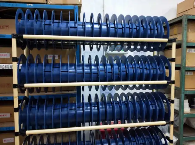
Products Specified for Semiconductor And IC Distribution
The items most often supplied into semiconductor and ic distribution.
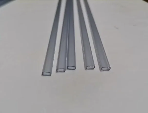
QFN, MLF, LPCC Tubes
These tubes are designed for QFN, MLF, and LPCC devices, providing ESD protection during semiconductor packaging, storage, and shipping.
View Details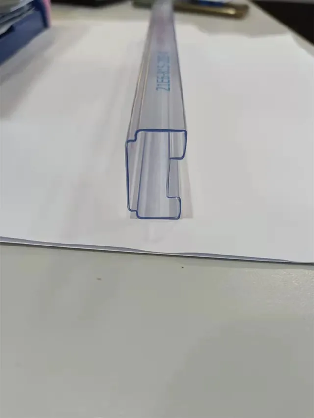
SOP, SSOP, TSSOP Tubes
SOP, SSOP, and TSSOP tubes are anti-static plastic shipping tubes designed for through-hole and surface-mount devices with narrow lead pitches and small body widths.
View Details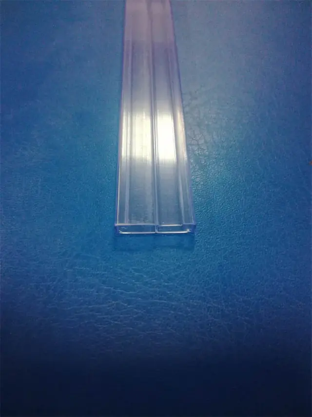
Anti-Static IC tubes for IC, SOP,DIP,TO-220,PLCC
Anti-Static IC Tubes are extruded plastic channels designed for packaging through-hole and surface-mount electronic components including ICs, SOP, DIP, TO-220, and PLCC packages.
View Details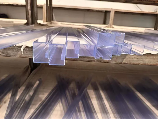
Anti Static Shipping Tubes
Anti Static Shipping Tubes are extruded plastic channels designed to protect electronic components from electrostatic discharge, mechanical shock, and environmental damage during transport and storage.
View Details
Color Anti-static Tubes
Color anti-static tubes are extruded plastic channels designed to hold electronic components in a fixed orientation from the component vendor to the pick and place machine.
View Details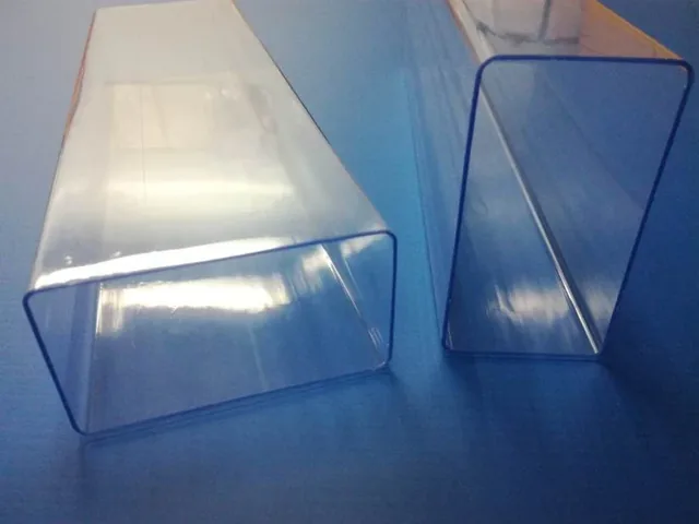
PLCC, LCC Tubes
PLCC and LCC tubes are extruded plastic channels designed to hold leaded and leadless chip carrier devices in a fixed orientation from component vendor to pick and place machine.
View DetailsTypical Jobs in Semiconductor And IC Distribution
- Re-packing bulk ICs into fixed-count anti-static tubes for distribution to downstream customers
- Shipping tested semiconductors from an assembly and test facility to an end customer with full traceability
- Storing buffer stock of high-risk allocation parts in anti-static tubes with consistent orientation
- Converting a device from bulk to tape and reel packaging for integration into an SMT production line
- Providing matching spare tubes for rework of returned or partially used reels to maintain process continuity
How a Semiconductor And IC Distribution Project Runs
- Submit device drawing, tube drawing, or a physical sample to match the exact profile
- Select material based on clarity, impact strength, and dimensional tolerance: PVC, PS, PC, PETG, or ABS
- Receive drawing for approval before tooling is cut, ensuring fit and function before production
- Mould making and tooling trial followed by 20-50 free sample tubes for fit and function testing
- Extrusion, cutting, anti-static treatment, plug fitting, and carton packing completed in-house
- Repeat orders run against approved tooling with 5-15 day lead time, depending on quantity
What Delivery Looks Like
- MOQ 10000 pieces for standard tube profiles
- Samples delivered in 3-5 days, stock profiles in 5-15 days depending on quantity
- Custom tooling: 25-day ARO for basic low volume, typically 4-6 weeks, 10-12 weeks for complex or high-volume tools
- Weekly capacity 50000 pcs, monthly output of finished products 150 tons
- Packing in cartons or to customer specification, T/T and L/C accepted
- Shipped from Shenzhen, Guangdong, China
Related Guides
Guides relevant to semiconductor and ic distribution.
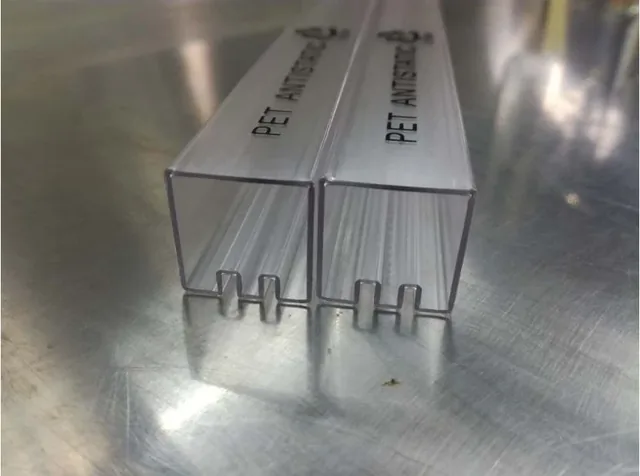
Custom IC Tubes For Specific Device Profiles
Each IC tube is extruded to match a unique device profile—shape, width, cavity depth and end plug type.
Read Guide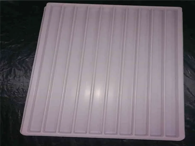
Vacuum Formed Trays For Component Packaging
Vacuum formed trays are made by heating a plastic sheet, stretching it over a mold, and pulling it down with vacuum pressure.
Read Guide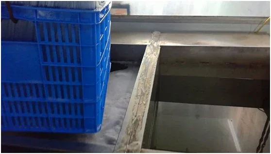
How Anti Static IC Tubes Are Made From PVC
The process starts with PVC resin fed into an extruder.
Read GuideSemiconductor And IC Distribution Questions
Can you match a package that has just been released?
Yes. Over a thousand open tools cover through-hole, SMT, and leadless packages including QFN, MLF, and LPCC. If no existing tool fits, a new profile is tooled from your drawing or a physical sample.
How tight is the tolerance for high speed loading?
Critical dimension control is within 5 mils on PVC and plus minus 2 mils, about 50 micron, on polycarbonate. The tighter grade is used where unattended loading must run without shingling.
Do you support both tube and tape and reel packaging?
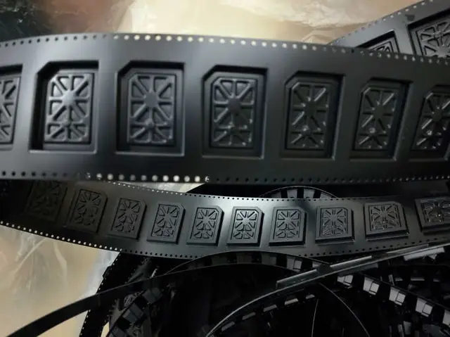
Yes. Tubes are used for larger or heavier bodies. Carrier tape and reel is produced for high-volume SMT placement of small SMD parts. Both are manufactured in-house.
What certification do you hold?
RoHS compliance on all products, ISO14001 as the quality management system, and full compliance with the Sony environmental protection requirement.
Will you take small quantities?
Small and large orders are both handled. However, the standard tube MOQ is 10000 pieces due to the cost of extrusion changeover, which must be recovered through run length.
Packaging Specified Around Your Semiconductor And IC Distribution Parts
Send the device list with quantities and the receiving line type. A format and a lead time come back within 24 hours.