Industry Application
Machine Vision For Semiconductor and IC
Character marking, pin geometry and wafer level defects on parts where the feature of interest is smaller than the tolerance you are allowed to miss.
Industry Pain Points
Why These Parts Are Hard To Image
- IC surface characters are laser marked with very low contrast against the package.
- Connector and QFP pin flatness has to be judged in three dimensions from a single view.
- Ceramic packages crack in ways that only show up under the right angle of incidence.
- Wafer level laser marks reflect specularly and wash out under ordinary front lighting.
Customer Requirements
Published Inspection Tasks
- Characters inspection of IC surface
- Characters inspection of the semiconductor products like IC
- IC charecter inspection
- IC Pin’s flatness inspection
- Flatness inspection of IC connector pin
- QFP and SOP inspection.
- Semiconductors defects inspection like IC
- LED wafer inspection
- Laser mark inspection of wafer
- Ceramic package things crack inspection.
- Characters inspection of ceramic condenser
- Damage inspection of condenser
Recommended Products
Component Ranges For This Industry
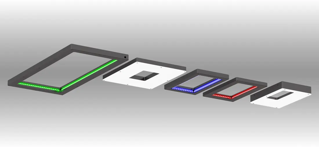
LED Lights
Angle Square Lights View Details →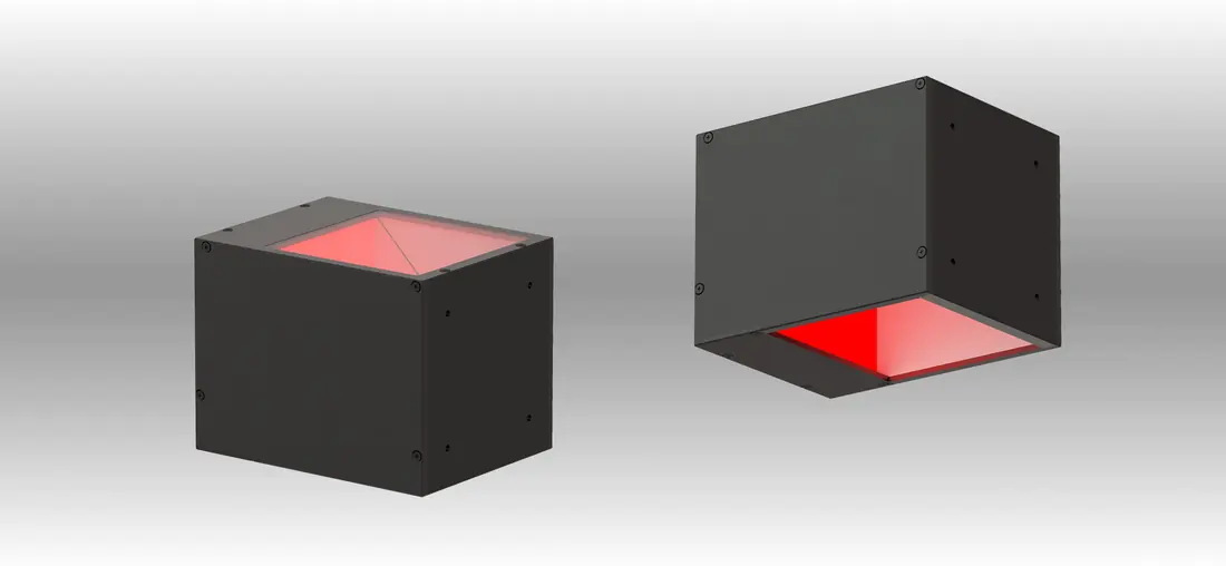
LED Lights
Coaxial Lights View Details →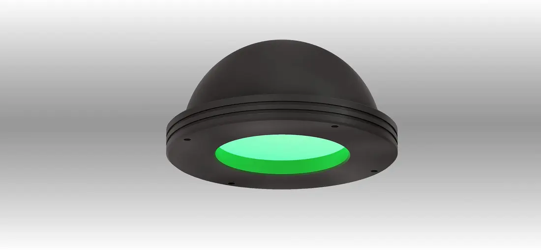
LED Lights
Dome Lights View Details →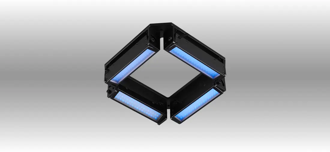
LED Lights
Bar Lights Combined View Details →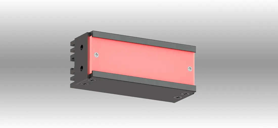
LED Lights
Bar Lights (3mm LED type) View Details →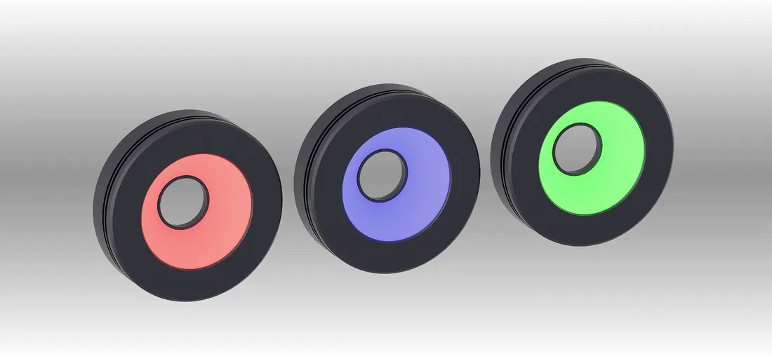
LED Lights
Low Angle Ring Lights View Details →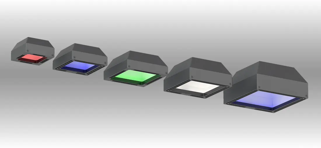
LED Lights
Square Dome Lights View Details →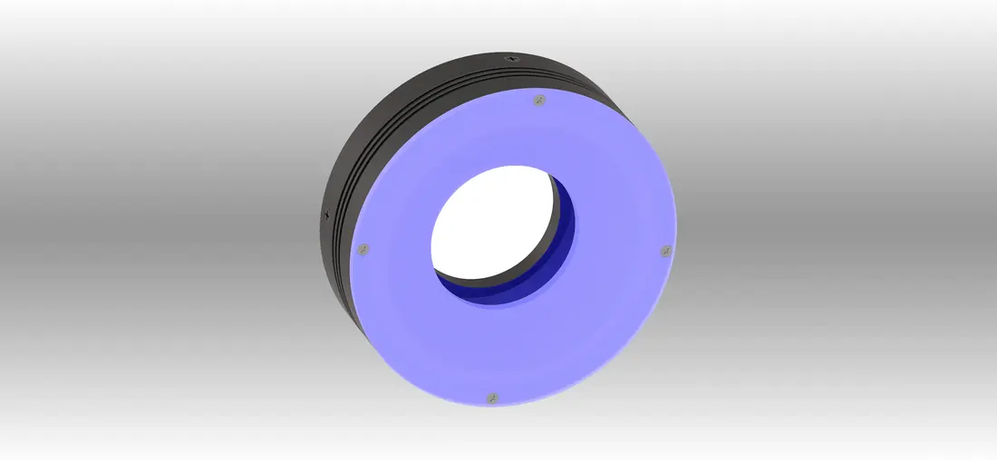
LED Lights
Ring Lights View Details →Solution Process
How A Project Runs From Enquiry To Delivery
Send The Part And The Target
A photo of the part, the defect you need to catch, the field of view and the line speed.
Lighting And Optics Proposal
Our design engineers propose a lighting geometry, a lens format and a camera that hold together as one chain.
Sample Or Custom Build
Standard parts ship from catalogue. Custom lighting samples are normally provided within 10 working days.
Validation On Your Part
You prove the image on the real part. Where the geometry needs changing, the design is revised before volume.
Supply And Repeat Orders
Once the model is fixed, repeat orders reference the same model number and the same imaging result.
Delivery Capability
What We Commit To
- More than 20 experienced customized design engineers for lighting and optics design.
- Most customised products provided within two weeks.
- Urgent customised demand shortened to around five days.
- Customised lighting samples normally provided within 10 working days.
- Most focal lenses shipped within three days.
- Lending samples for test available on the telecentric line scan lens range.
Every figure above is taken from published SBS Vision material.
Related
Solutions And Technical Reading
Custom Lighting and Optics Design
More than 20 lighting and optics design engineers, most custom products delivered within two weeks and urgent builds inside five days.
Structured Light 3D and Curved Surface Inspection
Structured lighting research aimed at parts where a flat two dimensional image cannot separate a real defect from a shadow.
High Speed Line Scan Imaging
Line scan illumination measured at more than one million lux, matched with 4K to 16K line scan optics for continuous web inspection.
Component Matching and Supply
Light, controller, lens and camera specified together as one imaging chain instead of four separate purchase lines.
FAQ
Semiconductor and IC FAQ
Which component range matters most for semiconductor and ic
Are these applications published or estimated
Can the lighting be designed for our exact part
How do I start
Send Us A Part From Your Line
One photo and one sentence about the defect is usually enough to get a lighting geometry suggestion back.