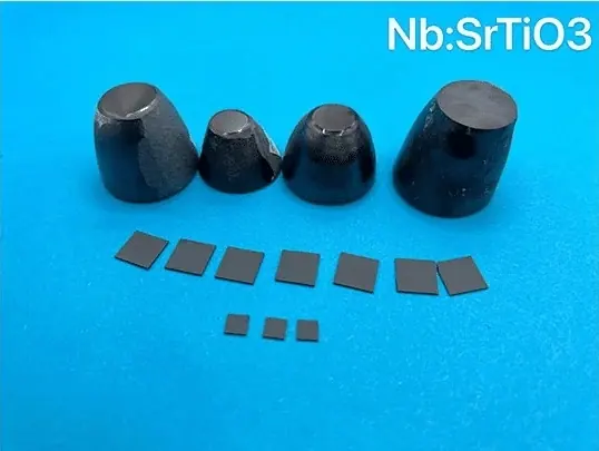

Niobium-doped strontium titanate has a similar structure to pure strontium titanate single crystal, but Nb:SrTiO3 has electrical conductivity. The conductive Nb:SrTiO3 substrates provide an electrode for certain thin film and device applications. At present, we can provide Nb:SrTiO3 single crystal substrates with Niobium doping concentration of: 0.1wt%, 0.5wt%, 0.7wt% and 1.0wt%. OST Photonics offers high quality Nb:...
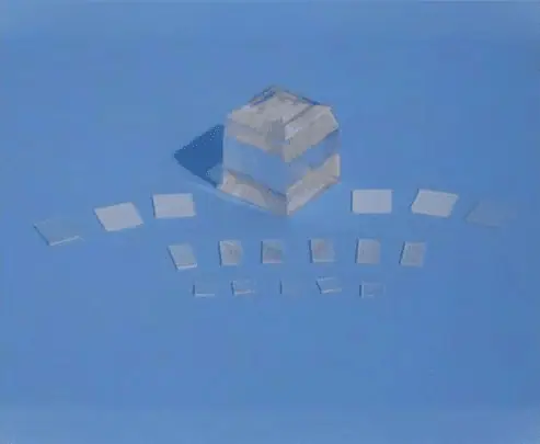
Niobium-doped strontium titanate has a similar structure to pure strontium titanate single crystal, but Nb:SrTiO3 has electrical conductivity. The conductive Nb:SrTiO3 substrates provide an electrode for certain thin film and device applications. At present, we can provide Nb:SrTiO3 single crystal substrates with Niobium doping concentration of: 0.1wt%, 0.5wt%, 0.7wt% and 1.0wt%.
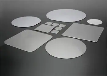
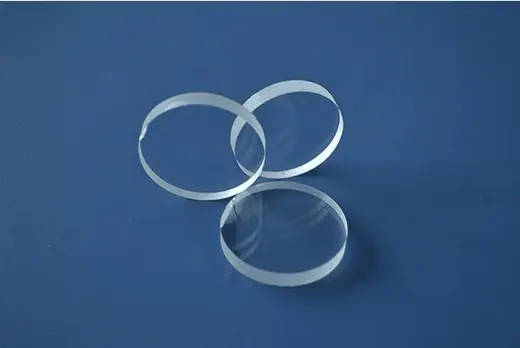
OST Photonics offers high quality Nb:SrTiO3 substrates for researchers and industries. Crystal orientation, size and thickness can be customized according to your requirements.
With superconductivity, semi-conductivity, gas sensitivity, heat sensitivity and photosensitivity
Low dielectric loss
High dispersion frequency
High dielectric constant
Nb:SrTiO3 substrates provide an electrode for certain thin film and device applications
Orientation: <100>,<110>,<111>, etc.
Dimension: 1”, 10x5mm, 10x10mm, 15x15mm, 20x20mm, etc.
Thickness: 0.5mm, 1.0mm, etc.
Available items: wafers, substrates, blanks and customized optics
Nb Concentration | 1.0wt% | 0.7wt% | 0.5wt% | 0.1wt% |
Resistivity | 0.0035 ohm.cm | 0.007 ohm.cm | 0.05 ohm.cm | 0.08 ohm.cm |
Mobility | 9.0 cm2/vs | 8.5 cm2/vs | 8.5 cm2/vs | 6.5 cm2/vs |
Orientation | <100>,<110>,<111>, etc. | |||
Orientation Tolerance | ±0.5° or better | |||
Dimension | 1”, 10x5mm, 10x10mm, 15x15mm, 20x20mm, etc. | |||
Dimension Tolerance | ±0.1 mm or better | |||
Thickness | 0.5mm, 1.0mm, etc. | |||
Thickness Tolerance | ±0.05 mm or better | |||
Surface Finish | Single side polished (SSP)/Double sides polished (DSP) | |||
Surface Roughness | Ra≤5Å (5µmx5µm) | |||
Package | Class 100 clean bag, Class 1000 super clean room | |||
The following specifications are listed on our original catalogue. Custom dimensions, orientations and surface finishes are produced to your drawing.
Send us your dimensions, orientation, surface finish and quantity. Our engineers reply with a technical proposal and price.