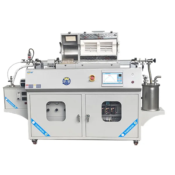
Low-Temperature (≤400°C) Deposition of High-Quality Dielectric and Passivation Films Using a 1200°C Dual-Zone PECVD System
1200°C dual-zone PECVD (Plasma-Enhanced Chemical Vapor Deposition) system provides a powerful and flexible solution, enabling excellent film quality at low substrate temperatures through precise thermal and plasma control. This article explores the process principles, film characteristics, and pract
- Laboratorydielectric thin filmsdual-zone PECVD systemlow-temperature PECVDpassivation layer deposition2025-12-26
Introduction
As device architectures continue to scale down and diversify, the demand for low-temperature deposition of high-quality dielectric and passivation films has become increasingly critical. Advanced applications such as flexible electronics, heterojunction solar cells, MEMS devices, and back-end semiconductor processing often impose strict thermal budgets, typically ≤400°C.
Conventional thermal CVD processes struggle to meet these requirements without sacrificing film density, uniformity, or electrical performance. In this context, the 1200°C dual-zone PECVD (Plasma-Enhanced Chemical Vapor Deposition) system provides a powerful and flexible solution, enabling excellent film quality at low substrate temperatures through precise thermal and plasma control.
This article explores the process principles, film characteristics, and practical advantages of using a high-temperature dual-zone PECVD system for low-temperature dielectric and passivation film deposition.
Fundamentals of PECVD Technology
PECVD relies on plasma to dissociate precursor gases into highly reactive radicals, allowing thin-film growth at significantly reduced substrate temperatures compared to thermal CVD. Typical dielectric materials deposited by PECVD include:
Silicon nitride (SiNx)
Silicon oxide (SiOx)
Silicon oxynitride (SiON)
Hydrogenated amorphous silicon (a-Si:H)
Why High-Temperature Capability Matters for Low-Temperature Deposition
Although the substrate temperature remains low, the 1200°C-rated heating zone plays a crucial role in film quality:
Efficient precursor decomposition: High temperatures ensure stable and complete dissociation of gases such as SiH₄, NH₃, N₂O, and O₂.
Improved plasma uniformity: Stable plasma chemistry reduces particle formation and compositional fluctuations.
Reduced hydrogen-related defects: Enhanced gas-phase reactions help minimize excessive hydrogen incorporation in the film.
As a result, films deposited at ≤400°C exhibit properties comparable to those produced at much higher substrate temperatures in conventional systems.
1. High Film Density and Low Defect Density
Dual-zone PECVD enables the formation of dense dielectric films with:
Low pinhole density
Reduced microvoids
Improved barrier properties
This is especially important for gate dielectrics and surface passivation layers where leakage current and reliability are critical.
2. Excellent Thickness Uniformity and Conformality
Optimized plasma distribution and gas flow design result in:
Thickness uniformity typically within ±2–3%
Good step coverage on structured or textured surfaces
Consistent refractive index across large substrates
These features are essential for semiconductor wafers and photovoltaic cells.
3. Tunable Film Stress
Film stress can be precisely adjusted by controlling:
Plasma power
Gas ratios (e.g., SiH₄/NH₃)
Substrate temperature
This enables low-stress or stress-balanced films, reducing the risk of cracking, delamination, or wafer bowing.
4. Superior Electrical and Passivation Performance
Low-temperature PECVD films deposited using a dual-zone system demonstrate:
High dielectric strength
Low leakage current
Excellent surface and bulk passivation
For example, SiNx films can achieve low surface recombination velocities, making them ideal for high-efficiency solar cells and advanced CMOS devices.
Semiconductor Manufacturing
Gate dielectrics and interlayer dielectrics
Passivation layers for CMOS and power devices
Back-end-of-line (BEOL) processing
Photovoltaics
SiNx passivation and anti-reflection coatings
Heterojunction and PERC solar cells
Thin-film photovoltaic technologies
Flexible and Organic Electronics
OLED encapsulation layers
Thin-film transistor (TFT) dielectrics
Wearable and bendable electronics
MEMS and Sensors
Electrical insulation layers
Environmental and chemical protection coatings
Stress-engineered functional films
Advantages for Research and Process Development
For R&D laboratories and pilot lines, a 1200°C dual-zone PECVD system offers:
Wide process window: Suitable for multiple materials and applications
High reproducibility: Stable plasma and temperature control
Scalability: Easy transition from research to small-scale production
Customization: Flexible configuration for different substrate sizes and gases
Conclusion
The 1200°C dual-zone PECVD system represents an advanced platform for low-temperature (≤400°C) deposition of high-quality dielectric and passivation films. By decoupling precursor activation from substrate heating, it delivers dense, uniform, low-defect films while preserving compatibility with temperature-sensitive substrates.
For researchers and engineers working in semiconductors, photovoltaics, MEMS, and flexible electronics, this technology provides an optimal balance between film performance, process flexibility, and thermal safety—making it an indispensable tool for next-generation device development.
Share this entry
You might also like
What is the Tube Furnace Tube Made Of? An In-Depth Analysis
What is the Use of Hydrogen in the Tube Furnace?
Factors Influencing the Price of CVD Reactors
Rotary Tube Furnace Price: Factors, Trends, and ZYLAB’s Advantage
Related ZYLAB Products
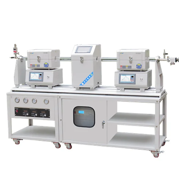
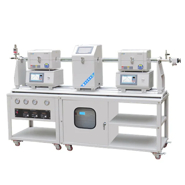
Dual-Furnace Sliding PECVD System for High-Precision Nanowire and Thin Film Deposition
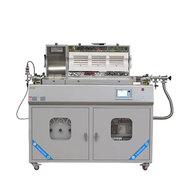
High-Performance Three-Zone PECVD System for Precision Thin Film Deposition
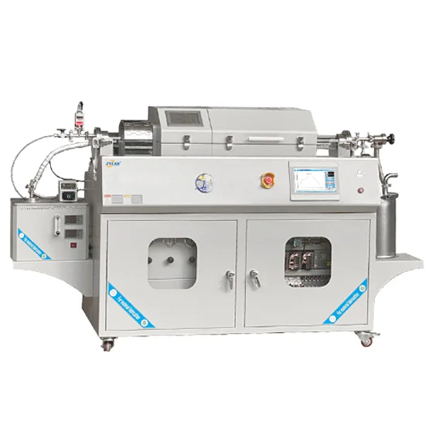
1200°C Dual-Zone PECVD System with Solid–Liquid Evaporation and Anti-Condensation Design, Featuring 4-Channel Gas Delivery
Fast Heating PECVD System for Rapid Thin Film Deposition
Working With ZYLAB On A Project Like This
How quickly can Low-Temperature (≤400°C) Deposition of High-Quality Dielectric and Pas be shipped?
Most standard ZYLAB models are held in stock. After testing and packing we normally ship Low-Temperature (≤400°C) Deposition of High-Quality Dielectric and Pas within 3 to 7 days. Customised builds are scheduled after the drawing is confirmed, and we give you the date in writing before the order is placed.
Can Low-Temperature (≤400°C) Deposition of High-Quality Dielectric and Pas be customised for our process?
Yes. Chamber or tube size, temperature profile, atmosphere, gas path, control system and data recording can all be adapted. Send us your process conditions and sample details and our engineers work out a configuration with you.
What warranty comes with Low-Temperature (≤400°C) Deposition of High-Quality Dielectric and Pas?
Most ZYLAB products carry a 2-year warranty, glass components excluded; the exact term for this model is the one printed in its specification table and repeated on the quotation. Within the warranty period any part that fails through no misuse of your own is replaced free of charge.
Can we get technical help before ordering Low-Temperature (≤400°C) Deposition of High-Quality Dielectric and Pas?
Yes, and it is free. Our technical staff help with model selection, troubleshooting, manuals and application questions whether or not you have ordered from us before. Write to [email protected] or message us on WhatsApp.
Have A Similar Requirement
Describe the material, the temperature and the throughput you need and an engineer will answer with a workable configuration.