Wafer Processing Techniques and Required Equipment
According to the requirements of different processes, equipment such as tube furnaces, heat treatment furnaces, and CVD systems must meet varying demands for temperature accuracy and uniformity.
- LaboratoryThermal ProcessingWafer AnnealingWafer DiffusionWafer Nitridation2024-12-25
Table of Contents
Wafer processing involves various techniques, typically requiring equipment capable of operating within specific temperature ranges.
Annealing
- Process Description: Annealing is used to modify the crystal structure of the wafer, repair material defects, and improve electrical properties.
- Temperature Range: Typically between 500°C and 1100°C.
Diffusion
- Process Description: The diffusion process introduces dopants (e.g., phosphorus, boron) into silicon wafers to achieve the desired semiconductor properties.
- Temperature Range: Approximately 800°C to 1200°C, depending on the type of dopant material.
Oxidation
- Process Description: Oxidation creates a layer of silicon dioxide (SiO₂) on the wafer surface, used for fabricating dielectric layers and isolation layers.
- Temperature Range: Usually between 800°C and 1100°C.
Thin Film Deposition
- Process Description: Thin film deposition coats the wafer surface, commonly using Chemical Vapor Deposition (CVD) or Physical Vapor Deposition (PVD).
- Temperature Range:
CVD: Typically between 400°C and 1000°C.
PVD: Generally lower, ranging from 200°C to 500°C.
Etching
- Process Description: Etching removes unwanted material from the wafer surface using chemical or physical methods to create micron-scale circuit patterns.
- Temperature Range: Usually at room temperature or slightly above, depending on the etching liquid or gas used.
Doping
- Process Description: Doping introduces external dopants into the wafer to alter its electrical conductivity. Common dopants include boron and phosphorus.
- Temperature Range: Typically between 800°C and 1100°C, depending on the diffusion rate of the dopant material.
Laser Annealing
- Process Description: Laser annealing rapidly heats the wafer surface, enabling precise control of annealing regions and temperatures.
- Temperature Range: Extremely high instantaneous temperatures, typically >1000°C, but with very short duration.
Chemical Mechanical Polishing (CMP)
- Process Description: CMP smoothens the wafer surface by removing thin films or oxide layers.
- Temperature Range: Usually conducted at room temperature, though slightly elevated temperatures may be used to accelerate certain chemical reactions.
Final Inspection Before Packaging
- Process Description: This process ensures the wafer meets quality standards, checking for material defects and pattern accuracy.
- Temperature Range: Usually conducted at room temperature.
Nitridation
- Process Description: Nitridation forms a silicon nitride layer on the wafer surface, improving thermal resistance, hardness, and stability.
- Temperature Range: Typically between 800°C and 1100°C.
Wafer Processing Temperature Requirements
For most wafer processing techniques, such as annealing, diffusion, oxidation, doping, and nitridation, high-temperature equipment typically needs to reach 1000°C to 1200°C.
For thin-film deposition, the temperature requirements are generally lower, usually ranging from 400°C to 800°C.
Laser annealing may require instantaneous temperatures exceeding 1000°C, but the processing time is extremely short.
Depending on the specific process requirements, equipment such as tube furnaces, thermal processing furnaces, and CVD systems must meet different demands for temperature accuracy and uniformity.
Share this entry
You might also like
Related ZYLAB Products
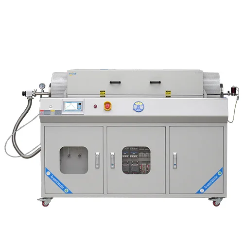
Multi-Zone High Temperature Quartz Tube Annealing Furnace for Wafer Processing
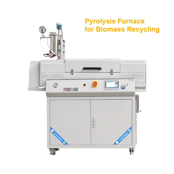
Advanced Continuous Pyrolyzers for Biomass and Organic Solid Waste Thermal Processing & Sintering
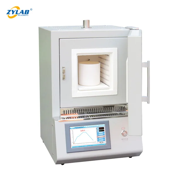
4.5L Muffle Furnace – Precision 1200°C Laboratory Furnace for Thermal Processing
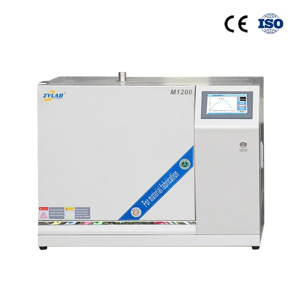
Economy Muffle Furnace | 1200°C Lab Furnace for Routine Thermal Processing
Working With ZYLAB On A Project Like This
Can Wafer Processing Techniques and Required Equipment be customised for our process?
Yes. Chamber or tube size, temperature profile, atmosphere, gas path, control system and data recording can all be adapted. Send us your process conditions and sample details and our engineers work out a configuration with you.
How quickly can Wafer Processing Techniques and Required Equipment be shipped?
Most standard ZYLAB models are held in stock. After testing and packing we normally ship Wafer Processing Techniques and Required Equipment within 3 to 7 days. Customised builds are scheduled after the drawing is confirmed, and we give you the date in writing before the order is placed.
How is Wafer Processing Techniques and Required Equipment packed for export?
Packing is chosen for the safety of the machine against freight cost, typically a plywood or wooden crate with internal padding and vacuum-sealed accessories. Export documents such as Form A, Form E and Form F can be issued to help you save duty.
Can you supply items that are not on this page?
Yes. We have access to the complete lines of most of our suppliers and build custom equipment in our own factory, so tell us what the experiment needs and we will source or make it.
Have A Similar Requirement
Describe the material, the temperature and the throughput you need and an engineer will answer with a workable configuration.