
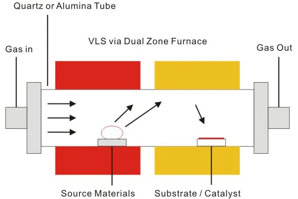
Chemical Vapour Deposition (CVD) Process Guide
Chemical Vapor Deposition (CVD) is a process used in the manufacturing of thin films, coatings, and other materials. It involves the deposition of a thin layer of material onto a substrate through the chemical reaction of gaseous precursors.
- LaboratoryThermal ProcessingAtmospheric pressure CVD (APCVD)Biomedical CVD applicationsChemical sensors CVD2024-01-05
Table of Contents
Chemical Vapor Deposition (CVD) is a process used in the manufacturing of thin films, coatings, and other materials. It involves the deposition of a thin layer of material onto a substrate through the chemical reaction of gaseous precursors.
The process takes place in a controlled environment, typically within a reaction chamber or furnace, where the substrate is exposed to the vaporized precursor chemicals.
1. Precursor Selection
Selecting appropriate precursor chemicals is crucial in CVD. These precursors should be volatile and easily vaporized at the process temperature.
2. Reaction Chamber
The substrate, which can be a wafer or another material, is placed inside a reaction chamber. This chamber is designed to control temperature, pressure, and other relevant parameters.
3. Vaporization
The selected precursor chemicals are vaporized, usually by heating them to their boiling or sublimation point. This results in the formation of a vapor phase.
4. Transport and Adsorption
The vaporized precursors are transported to the substrate surface, where they come into contact and adsorb onto the substrate.
5. Chemical Reaction
Upon adsorption, chemical reactions take place on the substrate surface. These reactions lead to the formation of a solid layer of the desired material.
6. Film Growth
The solid material formed by the chemical reactions continues to grow on the substrate surface, creating a thin film.
7. By-Products Removal
Any by-products or unreacted precursors are removed from the reaction chamber.
8. Film Characteristics
The properties of the deposited film, such as thickness, composition, and structure, can be controlled by adjusting parameters like temperature, pressure, and precursor concentrations.
CVD is widely used in various industries for the production of thin films for electronic devices, optical coatings, protective coatings, and more. It offers advantages such as high purity, uniformity, and the ability to coat complex shapes and structures.
Different variations of CVD, such as atmospheric pressure CVD (APCVD) and low-pressure CVD (LPCVD), exist to accommodate specific requirements of different applications.
Applications
Chemical Vapor Deposition (CVD) finds applications in a variety of industries due to its ability to produce thin films and coatings with precise control over properties like thickness, composition, and uniformity. Some of the key applications of CVD include:
1. Semiconductor Manufacturing
CVD is extensively used in the semiconductor industry to deposit thin films on silicon wafers. It is employed for the production of various layers, such as silicon dioxide (SiO2), silicon nitride (Si3N4), and polysilicon, used in the fabrication of integrated circuits and other semiconductor devices.
2. Thin Film Solar Cells
In the production of thin film solar cells, CVD is used to deposit layers of semiconductor materials like amorphous silicon, cadmium telluride (CdTe), or copper indium gallium selenide (CIGS) on substrates to create photovoltaic devices.
3. Optical Coatings
CVD is employed to deposit anti-reflective coatings, dielectric coatings, and other optical films on lenses, mirrors, and other optical components to enhance their performance and durability.
4. Hard Coatings and Wear Resistance
CVD is used to deposit hard coatings such as diamond-like carbon (DLC) or titanium nitride (TiN) on cutting tools, drills, and various mechanical components to improve wear resistance and durability.
5. Corrosion Protection
CVD is utilized to apply corrosion-resistant coatings on metal surfaces, providing protection against environmental factors and extending the lifespan of components in harsh conditions.
6. Microelectronics and MEMS (Micro-Electro-Mechanical Systems)
CVD is crucial in the fabrication of microelectronics and MEMS devices, where it is used to deposit thin films for insulation, passivation, and structural layers.
7. Chemical Sensors
CVD can be employed to create thin films for chemical sensors, enhancing their sensitivity and selectivity in detecting specific gases or chemicals.
8. Biomedical Applications
CVD is utilized in biomedical applications for coating medical implants with biocompatible materials to improve their integration with the body and reduce the risk of rejection.
9. Barrier Coatings
CVD is used to create thin films with barrier properties, preventing the permeation of gases and liquids. This is important in applications such as packaging for electronics and food.
10. Superconductors
CVD is employed in the production of high-temperature superconductors, where thin films of superconducting materials are deposited on substrates for use in electronic and magnetic devices.
These applications highlight the versatility of CVD in various industries, making it a critical technology for the development of advanced materials and devices.
Related ZYLAB Products
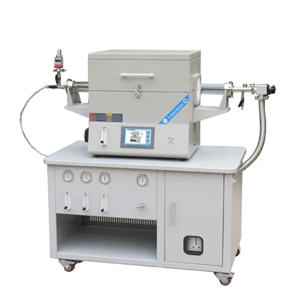
Chemical Vapor Deposition (CVD) System
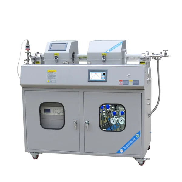
Advanced Plasma-Enhanced Chemical Vapor Deposition PECVD Furnace System
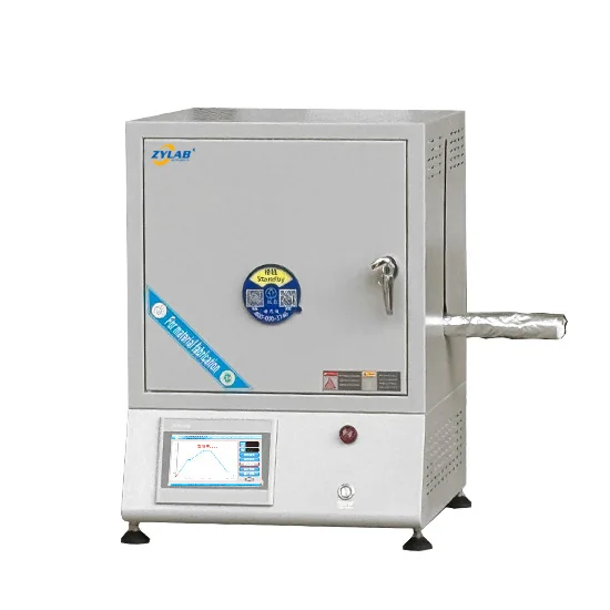
High-Pressure Hydrogen Preheating and Purge System for Laboratory Applications
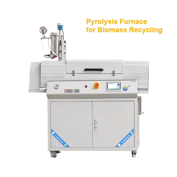
Advanced Continuous Pyrolyzers for Biomass and Organic Solid Waste Thermal Processing & Sintering
Working With ZYLAB On A Project Like This
What warranty comes with Chemical Vapour Deposition (CVD) Process Guide?
Most ZYLAB products carry a 2-year warranty, glass components excluded; the exact term for this model is the one printed in its specification table and repeated on the quotation. Within the warranty period any part that fails through no misuse of your own is replaced free of charge.
Can we get technical help before ordering Chemical Vapour Deposition (CVD) Process Guide?
Yes, and it is free. Our technical staff help with model selection, troubleshooting, manuals and application questions whether or not you have ordered from us before. Write to [email protected] or message us on WhatsApp.
Which shipping methods do you use?
Sea freight for consignments over about 60 kg (11-30 days to North America, 25-33 days to Europe, 7-20 days to Southeast Asia), air freight to airport in roughly 7-10 days, and DHL, FedEx or UPS door to door in about 5-7 days for small urgent items.
How can we pay for Chemical Vapour Deposition (CVD) Process Guide?
Bank (wire) transfer, letter of credit for larger orders, major credit and debit cards, and PayPal. Bank details are printed on the invoice; send us the transfer confirmation and we start processing straight away.
Have A Similar Requirement
Describe the material, the temperature and the throughput you need and an engineer will answer with a workable configuration.