Advancing Key Material Research with Ultrasonic Atomization CVD
The development of high-performance functional materials is critical for flexible electronics and next-generation energy devices. Flexible transparent conductive films (TCFs) and electrode functional layers are foundational for wearable devices, foldable displays, batteries, supercapacitors, and sol
- LaboratoryThermal Processingelectrode functional layersenergy materials researchflexible transparent conductive film2025-11-14
Table of Contents
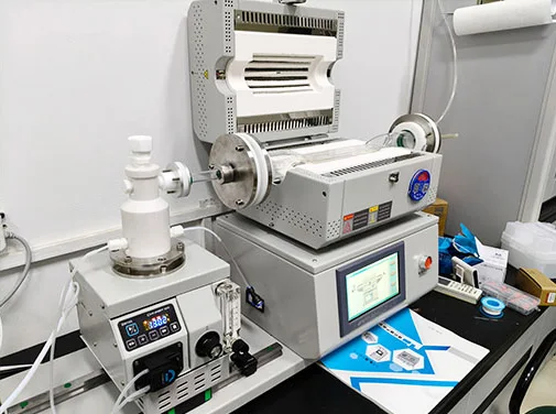
The development of high-performance functional materials is critical for flexible electronics and next-generation energy devices. Flexible transparent conductive films (TCFs) and electrode functional layers are foundational for wearable devices, foldable displays, batteries, supercapacitors, and solar cells. Achieving uniform, defect-free coatings with precise control over composition and microstructure is challenging. Ultrasonic Atomization Chemical Vapor Deposition (CVD) provides a precise solution for laboratory-scale material research.
How Ultrasonic Atomization CVD Works
- Precursor Solution Preparation: Dissolve target material precursors in a suitable solvent.
Ultrasonic Atomization: High-frequency vibrations generate fine droplets of the precursor solution.
Transport and Deposition: Droplets are carried to the heated substrate in a controlled atmosphere.
Thin-Film Formation: Solvent evaporates and precursor reacts/decomposes, forming uniform thin films.
This process ensures high uniformity and fine control over film morphology, thickness, and composition.
Precision Deposition for Flexible Transparent Conductive Films
Flexible TCFs—such as silver nanowires, graphene, and conductive oxides—require uniform deposition to maintain both transparency and conductivity while remaining mechanically flexible. Ultrasonic atomization enables:
Micrometer-scale precursor droplets for homogeneous coating.
Controlled growth parameters: film thickness, surface morphology, and conductivity can be precisely tuned.
Substrate-friendly deposition: gentle process suitable for polymers and other delicate flexible materials.
This level of control supports high-performance TCFs for wearable electronics, foldable displays, touch panels, and smart windows.
Functional Electrode Layers for Energy Devices
High-quality electrode layers are essential in lithium-ion/sodium-ion batteries, supercapacitors, and perovskite solar cells. Ultrasonic atomization CVD provides:
Consistent active material coating, reducing defects and enhancing reproducibility.
Multilayer and composite deposition: doped layers, heterostructures, and nanocomposites can be fabricated.
Optimized microstructure: tailored porosity and morphology improve ionic/electronic transport and cycling stability.
Advantages for Materials Research
Ultrasonic atomization CVD systems provide several key benefits for laboratory research:
High reproducibility: Critical for both fundamental studies and pre-industrial prototyping.
Flexibility in deposition parameters: Adjustable ultrasonic frequency, precursor concentration, substrate temperature, and deposition duration.
Broad material and substrate compatibility: Supports polymers, glass, metal foils, and complex substrate geometries.
Scalability for pilot studies: Enables seamless transition from small-scale experiments to larger-area coatings.
These features make ultrasonic atomization CVD particularly valuable for interdisciplinary materials research, including flexible electronics, optoelectronics, energy storage, and catalysis.
Conclusion
Ultrasonic atomization CVD provides precision, uniformity, and reproducibility required for cutting-edge material research. For flexible transparent conductive films, it ensures high transparency and conductivity on sensitive substrates. For energy device electrodes, it allows fine control over composition and microstructure to enhance performance.
By enabling the precise engineering of thin films and functional layers, ultrasonic atomization CVD accelerates innovation in next-generation electronics and energy technologies.
Share this entry
You might also like
Ultimate Guide to Glass Reactors: Types, Features, and Applications
Rotary Evaporator
Pouch Cell Preparation
Vacuum Filter
Related ZYLAB Products
Ultrasonic Atomization Pyrolysis CVD System
Advanced Continuous Pyrolyzers for Biomass and Organic Solid Waste Thermal Processing & Sintering
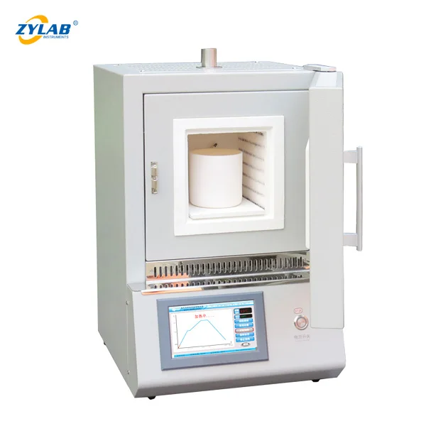
4.5L Muffle Furnace – Precision 1200°C Laboratory Furnace for Thermal Processing
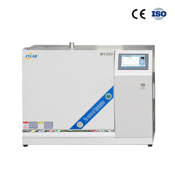
Economy Muffle Furnace | 1200°C Lab Furnace for Routine Thermal Processing
Working With ZYLAB On A Project Like This
How quickly can Advancing Key Material Research with Ultrasonic Atomization CVD be shipped?
Most standard ZYLAB models are held in stock. After testing and packing we normally ship Advancing Key Material Research with Ultrasonic Atomization CVD within 3 to 7 days. Customised builds are scheduled after the drawing is confirmed, and we give you the date in writing before the order is placed.
Is there a minimum order quantity for Advancing Key Material Research with Ultrasonic Atomization CVD?
No. ZYLAB has no minimum order requirement, so a single unit of Advancing Key Material Research with Ultrasonic Atomization CVD is a normal order. Occasionally a component supplier imposes a minimum quantity of their own, and we tell you as soon as we are notified.
Can we get technical help before ordering Advancing Key Material Research with Ultrasonic Atomization CVD?
Yes, and it is free. Our technical staff help with model selection, troubleshooting, manuals and application questions whether or not you have ordered from us before. Write to [email protected] or message us on WhatsApp.
What if Advancing Key Material Research with Ultrasonic Atomization CVD is damaged in transit?
Contact your ZYLAB sales engineer immediately with photographs. We arrange a substitute delivery promptly and handle the claim with the carrier.
Have A Similar Requirement
Describe the material, the temperature and the throughput you need and an engineer will answer with a workable configuration.