
Why Does Monocrystalline Silicon Require Annealing?
The primary purpose of annealing is to improve the crystal quality of monocrystalline silicon, relieve internal stress, repair defects, and optimize its physical and electronic properties, thereby meeting the application requirements in the semiconductor and photovoltaic fields.
- LaboratoryThermal ProcessingAnnealing FurnaceAnnealing of Monocrystalline MaterialsBenefits of Silicon Annealing2024-11-21
What Is Monocrystalline Silicon Annealing?
Monocrystalline silicon annealing is a heat treatment process in which the material is heated to a specific temperature, held in a controlled environment for a certain duration, and then slowly cooled.
The primary purpose of annealing is to improve the crystal quality of monocrystalline silicon, relieve internal stress, repair defects, and optimize its physical and electronic properties, thereby meeting the application requirements in the semiconductor and photovoltaic fields.
Relieving Internal Stress
During the growth, slicing, and processing of monocrystalline silicon, internal stresses may develop, leading to crystal deformation or defects. Annealing rearranges atoms through heating, relieving stress and restoring crystal integrity.
Repairing Crystal Defects
Crystal defects such as dislocations, micro-cracks, and vacancies can occur during the growth process of monocrystalline silicon. Annealing promotes the diffusion of silicon atoms, reducing or eliminating these defects and enhancing structural integrity.
Increasing Carrier Lifetime
Annealing reduces impurity concentrations and defect densities in silicon, lowering the recombination probability of carriers during migration and thereby improving carrier lifetime.
Regulating Dopant Distribution
In semiconductor device fabrication, annealing enables dopant atoms to redistribute within the silicon crystal, forming a uniform doping concentration to meet device performance requirements.
Improving Surface and Interface Quality
Annealing helps reduce oxide layers and other contaminants on the surface of monocrystalline silicon, improving surface flatness and interface quality, which optimizes device performance.
Heating Phase
The temperature typically ranges from 600°C to 1200°C, depending on the purpose and desired effects of annealing.
The heating rate must be controlled to prevent thermal stress caused by rapid temperature increases.
Holding Phase
The material is maintained at the target temperature for a certain period (ranging from minutes to hours) to ensure thorough repair of defects or stress within the silicon.
Cooling Phase
The material is cooled gradually to avoid thermal shock, which could introduce new stress or cracks.
Atmosphere Control
Annealing is usually conducted in an inert gas environment (e.g., argon or nitrogen), under vacuum, or in an oxygen atmosphere, depending on the specific annealing goals.
In the photovoltaic field, a hydrogen environment may be used to further passivate surface defects in the silicon.
Rapid Thermal Annealing (RTA)
This method involves rapid heating and cooling, making it suitable for adjusting dopant distribution or activating dopant atoms.
Conventional Annealing
Characterized by slower temperature changes and longer durations, it is used to relieve stress and repair crystal defects.
Hydrogen Annealing
Conducted in a hydrogen-containing atmosphere, this process passivates defects in silicon and enhances the photoelectric conversion efficiency of photovoltaic materials.
Reduction in Crystal Defect Density
Enhances the material’s crystalline integrity, making it more suitable for producing high-efficiency devices.
Improvement in Carrier Mobility
Reduces the interference from impurities and defects within the crystal, enhancing the mobility of electrons or holes.
Better Surface Passivation
For photovoltaic applications, annealing passivates surface defects, reducing surface recombination losses and improving efficiency.
Enhanced Mechanical Properties
Eliminating residual stress significantly improves the material’s crack resistance and processability.
Semiconductor Industry
Used in the production of integrated circuits, transistors, and other devices to enhance material performance and improve production yield.
Photovoltaic Industry
Boosts the photoelectric conversion efficiency of monocrystalline silicon solar cells, with widespread use in advanced cell technologies such as PERC and HJT.
Sensors and MEMS Devices
Enhances the reliability and sensitivity of silicon-based sensors and microelectromechanical systems (MEMS).
Through annealing, monocrystalline silicon undergoes significant structural and performance optimization, laying a solid foundation for its applications in high-tech industries.
Share this entry
You might also like
Related ZYLAB Products
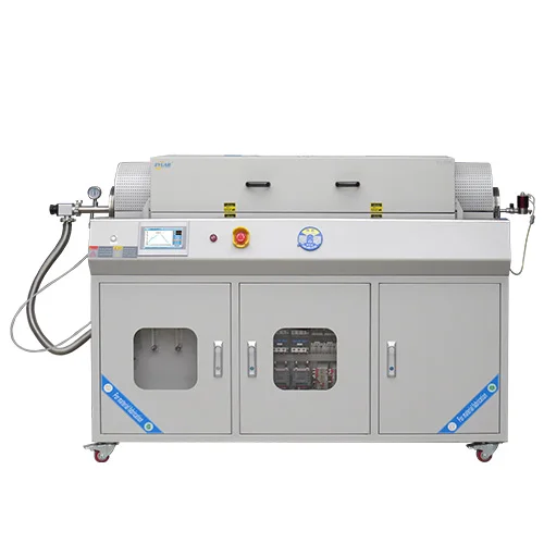
Multi-Zone High Temperature Quartz Tube Annealing Furnace for Wafer Processing
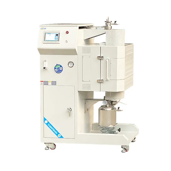
1700°C Vertical Atmosphere Controlled Quenching Furnace for High-Performance Heat Treatment
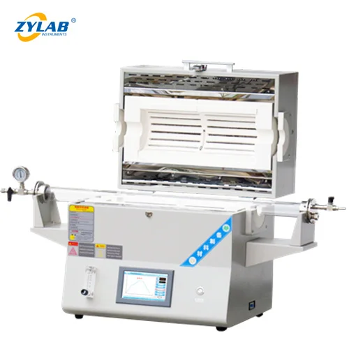
Customizable Tube Furnace with Gas Control System – Precision Atmosphere Processing
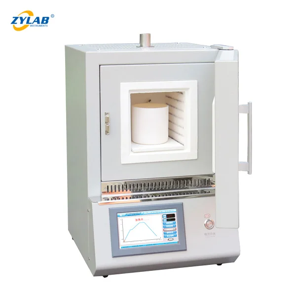
4.5L Muffle Furnace – Precision 1200°C Laboratory Furnace for Thermal Processing
Working With ZYLAB On A Project Like This
What warranty comes with Why Does Monocrystalline Silicon Require Annealing??
Most ZYLAB products carry a 2-year warranty, glass components excluded; the exact term for this model is the one printed in its specification table and repeated on the quotation. Within the warranty period any part that fails through no misuse of your own is replaced free of charge.
Can we get technical help before ordering Why Does Monocrystalline Silicon Require Annealing??
Yes, and it is free. Our technical staff help with model selection, troubleshooting, manuals and application questions whether or not you have ordered from us before. Write to [email protected] or message us on WhatsApp.
Which shipping methods do you use?
Sea freight for consignments over about 60 kg (11-30 days to North America, 25-33 days to Europe, 7-20 days to Southeast Asia), air freight to airport in roughly 7-10 days, and DHL, FedEx or UPS door to door in about 5-7 days for small urgent items.
How can we pay for Why Does Monocrystalline Silicon Require Annealing??
Bank (wire) transfer, letter of credit for larger orders, major credit and debit cards, and PayPal. Bank details are printed on the invoice; send us the transfer confirmation and we start processing straight away.
Have A Similar Requirement
Describe the material, the temperature and the throughput you need and an engineer will answer with a workable configuration.