
Product category
HDI PCB
High density interconnects (HDI) PCB
High density interconnects (HDI) PCB represent one of the fastest-growing technologies in PCBs. Because of its higher circuitry density than traditional circuit boards, the HDI PCB design is able to incorporate smaller vias and capture pads, and higher connection pad densities.
Advantages of HDI PCB
- Can reduce the cost of PCB: When the density of the PCB increases by more than eight layers, HDI PCB is used to make 2, 2, and the cost will be lower than the traditional complicated lamination process.
- Increase circuit density: the interconnection of traditional circuit boards and parts
- Conducive to the use of advanced construction technology
- With better electrical performance and signal accuracy
- Better reliability
- Can improve thermal properties
- Can improve radio frequency interference / electromagnetic wave interference / electrostatic discharge (RFI / EMI / ESD)
- Increase design efficiency
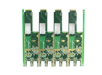
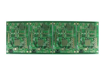
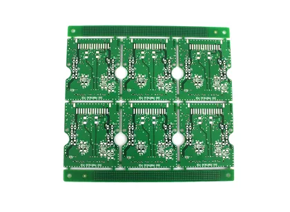
HDI PCB — Questions Buyers Ask
How many HDI PCB items are listed
3 boards are listed in this category. Every one shows its base material, layer count, board thickness, copper thickness, surface finish, minimum line width and spacing and minimum hole size.
How many layers can SiYi build
1~48 layer. Board thickness runs from 0.075mm to 14.0mm, the smallest hole is 0.1mm and the aspect ratio is 16:1.
Is there a minimum order quantity
No MOQ limited. Prototypes, quick turn and high volume production are all accepted.
How fast can boards be delivered
At the fastest, 24hr for L2, 48hr for L4~L6 and 72hr for L8 or more. Monthly capacity is 30,000 sq.meter and 4,500 varieties.
How quickly will I get a quote
Quote in 1 day.
Talk to a PCB Engineer
Send your Gerber on RS-274X and we will come back with a quote in 1 day.